LM317BT 查看數據表(PDF) - ON Semiconductor
零件编号
产品描述 (功能)
生产厂家
LM317BT Datasheet PDF : 12 Pages
| |||
LM317, NCV317
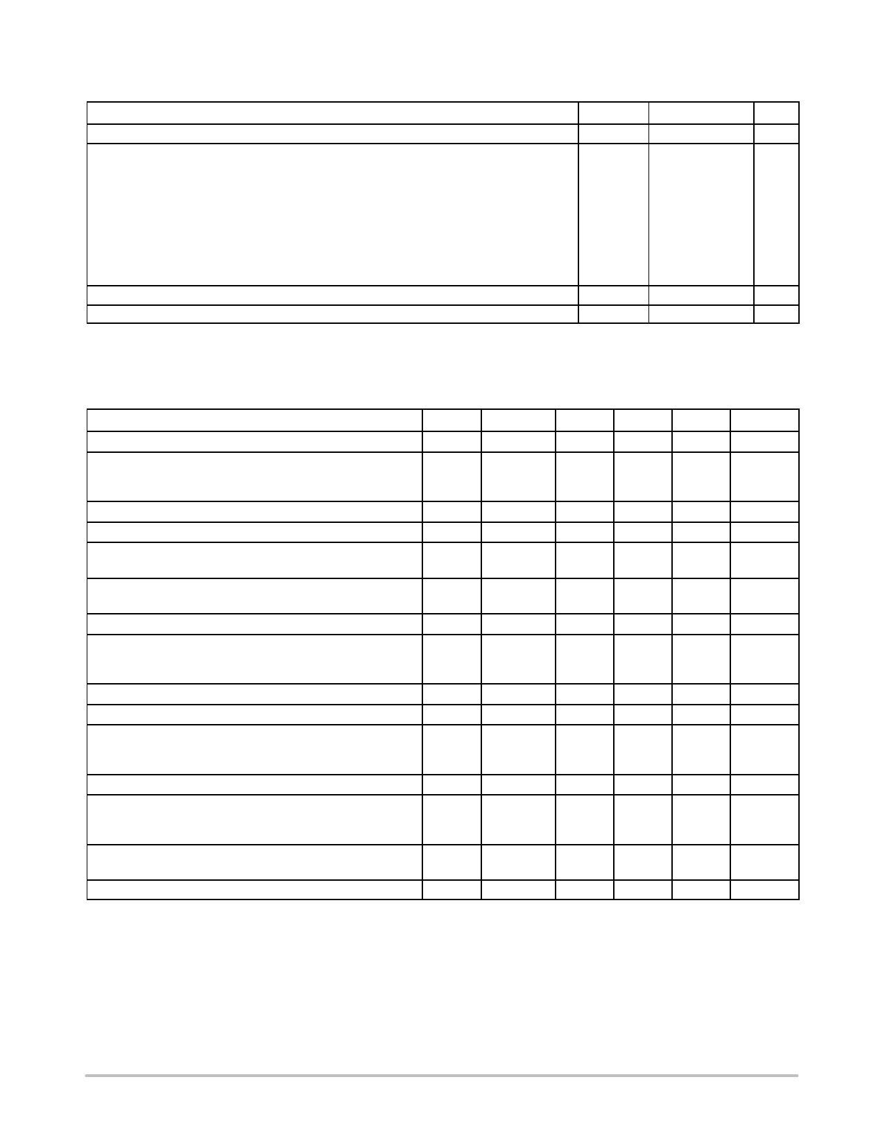
MAXIMUM RATINGS
Rating
Symbol
Value
Unit
Input−Output Voltage Differential
VI−VO
40
Vdc
Power Dissipation
Case 221A
TA = +25°C
Thermal Resistance, Junction−to−Ambient
Thermal Resistance, Junction−to−Case
Case 936 (D2PAK−3)
TA = +25°C
Thermal Resistance, Junction−to−Ambient
Thermal Resistance, Junction−to−Case
PD
Internally Limited W
qJA
65
°C/W
qJC
5.0
°C/W
PD
Internally Limited W
qJA
70
°C/W
qJC
5.0
°C/W
Operating Junction Temperature Range
TJ
−55 to +150
°C
Storage Temperature Range
Tstg
−65 to +150
°C
Stresses exceeding Maximum Ratings may damage the device. Maximum Ratings are stress ratings only. Functional operation above the
Recommended Operating Conditions is not implied. Extended exposure to stresses above the Recommended Operating Conditions may affect
device reliability.
ELECTRICAL CHARACTERISTICS (VI−VO = 5.0 V; IO = 0.5 A for D2T and T packages; TJ = Tlow to Thigh (Note 1); Imax and Pmax
(Note 2); unless otherwise noted.)
Characteristics
Figure Symbol
Min
Typ
Max
Unit
Line Regulation (Note 3), TA = +25°C, 3.0 V ≤ VI−VO ≤ 40 V
1
Load Regulation (Note 3), TA = +25°C, 10 mA ≤ IO ≤ Imax
2
VO ≤ 5.0 V
VO ≥ 5.0 V
Thermal Regulation, TA = +25°C (Note 4), 20 ms Pulse
Adjustment Pin Current
3
Adjustment Pin Current Change, 2.5 V ≤ VI−VO ≤ 40 V,
1, 2
10 mA ≤ IL ≤ Imax, PD ≤ Pmax
Reference Voltage, 3.0 V ≤ VI−VO ≤ 40 V,
3
10 mA ≤ IO ≤ Imax, PD ≤ Pmax
Line Regulation (Note 3), 3.0 V ≤ VI−VO ≤ 40 V
1
Load Regulation (Note 3), 10 mA ≤ IO ≤ Imax
2
VO ≤ 5.0 V
VO ≥ 5.0 V
Temperature Stability (Tlow ≤ TJ ≤ Thigh)
3
Minimum Load Current to Maintain Regulation (VI−VO = 40 V)
3
Maximum Output Current
3
VI−VO ≤ 15 V, PD ≤ Pmax, T Package
VI−VO = 40 V, PD ≤ Pmax, TA = +25°C, T Package
RMS Noise, % of VO, TA = +25°C, 10 Hz ≤ f ≤ 10 kHz
Ripple Rejection, VO = 10 V, f = 120 Hz (Note 5)
4
Without CAdj
CAdj = 10 mF
Long−Term Stability, TJ = Thigh (Note 6), TA = +25°C for
3
Endpoint Measurements
Regline
Regload
Regtherm
IAdj
DIAdj
Vref
Regline
Regload
TS
ILmin
Imax
N
RR
S
−
−
−
−
−
−
1.2
−
−
−
−
−
1.5
0.15
−
−
66
−
0.01
5.0
0.1
0.03
50
0.2
1.25
0.02
20
0.3
0.7
3.5
2.2
0.4
0.003
65
80
0.3
0.04
%/V
25
mV
0.5
% VO
0.07
% VO/W
100
mA
5.0
mA
1.3
V
0.07
%V
70
mV
1.5
% VO
−
% VO
10
mA
A
−
−
−
% VO
dB
−
−
1.0
%/1.0 k
Hrs.
Thermal Resistance Junction−to−Case, T Package
RqJC
−
5.0
−
°C/W
1. Tlow to Thigh = 0° to +125°C, for LM317T, D2T. Tlow to Thigh = − 40° to +125°C, for LM317BT, BD2T, Tlow to Thigh = − 55° to +150°C, for
NCV317BT, BD2T.
2. Imax = 1.5 A, Pmax = 20 W
3. Load and line regulation are specified at constant junction temperature. Changes in VO due to heating effects must be taken into account
separately. Pulse testing with low duty cycle is used.
4. Power dissipation within an IC voltage regulator produces a temperature gradient on the die, affecting individual IC components on the die.
These effects can be minimized by proper integrated circuit design and layout techniques. Thermal Regulation is the effect of these
temperature gradients on the output voltage and is expressed in percentage of output change per watt of power change in a specified time.
5. CAdj, when used, is connected between the adjustment pin and ground.
6. Since Long−Term Stability cannot be measured on each device before shipment, this specification is an engineering estimate of average
stability from lot to lot.
http://onsemi.com
2
Share Link: 