NCV4275ADS33R4G 查看數據表(PDF) - ON Semiconductor
零件编号
产品描述 (功能)
生产厂家
NCV4275ADS33R4G Datasheet PDF : 19 Pages
| |||
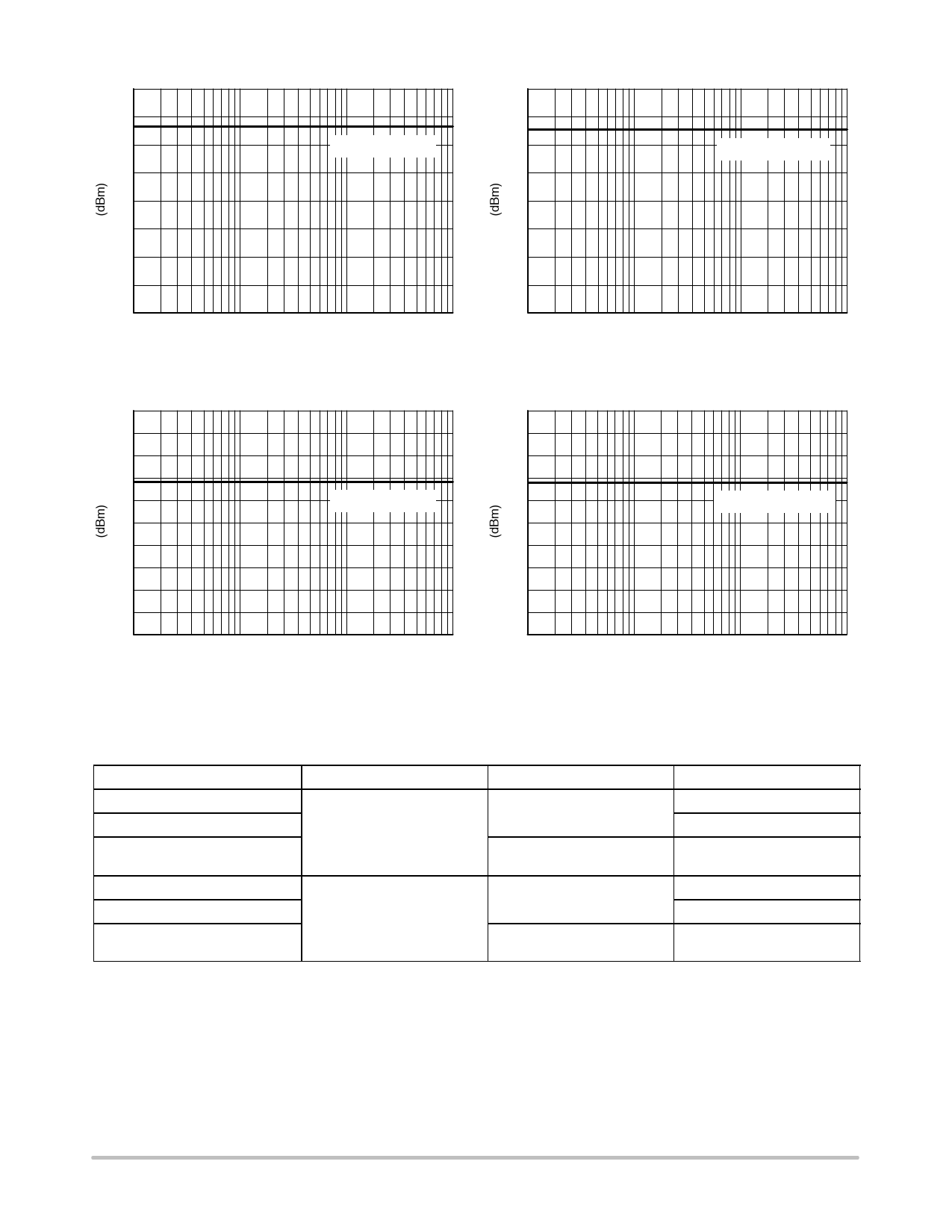
NCV4275A
40
40
30
Vin Pass 33 dBm
30
Vout Pass 33 dBm
20
20
10
10
0
1
10
100
1000
FREQUENCY (MHz)
Figure 35. Typical Vin Pin Susceptibility
25
20
15
RO Pass 17 dBm
10
5
0
1
10
100
1000
FREQUENCY (MHz)
Figure 37. Typical RO Pin Susceptibility
0
1
10
100
1000
FREQUENCY (MHz)
Figure 36. Typical Vout Pin Susceptibility
25
20
15
Delay Pass 17 dBm
10
5
0
1
10
100
1000
FREQUENCY (MHz)
Figure 38. Typical Delay Pin Susceptibility
ORDERING INFORMATION
Device
Output Voltage
Package
Shipping†
NCV4275ADS50G
NCV4275ADS50R4G
5.0 V
D2PAK
(Pb−Free)
50 Units/Rail
800 Tape & Reel
NCV4275ADT50RKG
DPAK
(Pb−Free)
2500 Tape & Reel
NCV4275ADS33G
NCV4275ADS33R4G
3.3 V
D2PAK
(Pb−Free)
50 Units/Rail
800 Tape & Reel
NCV4275ADT33RKG
DPAK
(Pb−Free)
2500 Tape & Reel
†For information on tape and reel specifications,including part orientation and tape sizes, please refer to our Tape and Reel Packaging
Specifications Brochure, BRD8011/D.
http://onsemi.com
17
Share Link: 