NE5210D 查看數據表(PDF) - Philips Electronics
零件编号
产品描述 (功能)
生产厂家
NE5210D Datasheet PDF : 14 Pages
| |||
Philips Semiconductors
Transimpedance amplifier (280MHz)
Product specification
NE5210
This represents the maximum limit attainable with the NE5210
operating at 200MHz bandwidth, with a half mark/half space digital
transmission at 850nm wavelength.
APPLICATION INFORMATION
Package parasitics, particularly ground lead inductances and
parasitic capacitances, can significantly degrade the frequency
response. Since the NE5210 has differential outputs which can feed
back signals to the input by parasitic package or board layout
capacitances, both peaking and attenuating type frequency
response shaping is possible. Constructing the board layout so that
Ground 1 and Ground 2 have very low impedance paths has
produced the best results. This was accomplished by adding a
ground-plane stripe underneath the device connecting Ground 1,
Pins 8–11, and Ground 2, Pins 1 and 2 on opposite ends of the
SO14 package. This ground-plane stripe also provides isolation
between the output return currents flowing to either VCC2 or Ground
2 and the input photodiode currents to flowing to Ground 1. Without
this ground-plane stripe and with large lead inductances on the
board, the part may be unstable and oscillate near 800MHz. The
easiest way to realize that the part is not functioning normally is to
measure the DC voltages at the outputs. If they are not close to their
+VCC
47µF
C1
C2
.01µF
quiescent values of 3.3V (for a 5V supply), then the circuit may be
oscillating. Input pin layout necessitates that the photodiode be
physically very close to the input and Ground 1. Connecting Pins 3
and 5 to Ground 1 will tend to shield the input but it will also tend to
increase the capacitance on the input and slightly reduce the
bandwidth.
As with any high-frequency device, some precautions must be
observed in order to enjoy reliable performance. The first of these is
the use of a well-regulated power supply. The supply must be
capable of providing varying amounts of current without significantly
changing the voltage level. Proper supply bypassing requires that a
good quality 0.1µF high-frequency capacitor be inserted between
VCC1 and VCC2, preferably a chip capacitor, as close to the package
pins as possible. Also, the parallel combination of 0.1µF capacitors
with 10µF tantalum capacitors from each supply, VCC1 and VCC2, to
the ground plane should provide adequate decoupling. Some
applications may require an RF choke in series with the power
supply line. Separate analog and digital ground leads must be
maintained and printed circuit board ground plane should be
employed whenever possible.
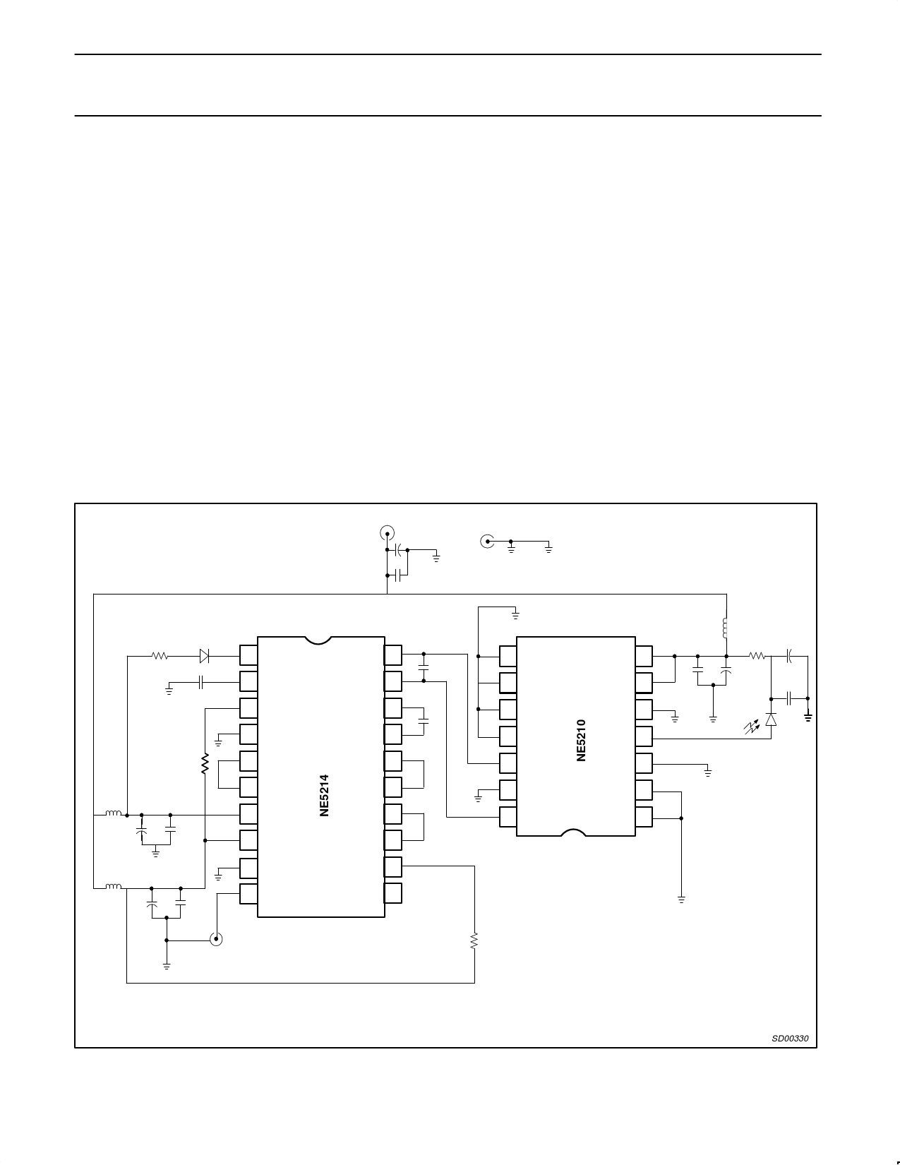
Figure 4 depicts a 50Mb/s TTL fiber-optic receiver using the BPF31,
850nm LED, the NE5210 and the NE5214 post amplifier.
GND
R2
D1
220
LED
C9
100pF
L2
10µH
C10
10µF
R3
47k
C11
.01µF
L3
10µH
C12
10µF
C13
.01µF
1 LED
2 CPKDET
3 THRESH
4 GNDA
5 FLAG
6 JAM
7 VCCD
8 VCCA
9 GNDD
10 TTLOUT
VOUT (TTL)
C7
IN1B 20
IN1A 19
CAZP 18
100pF
C8
CAZN 17 0.1µF
OUT1B 16
IN8B 15
OUT1A 14
IN8A 13
RHYST 12
RPKDET 11
8 GND
9 GND
10 GND
11 GND
12 OUT
13 GND
14 OUT
R4
4k
VCC 7
VCC 6
NC 5
IIN 4
NC 3
GND 2
GND 1
L1
10µH
R1
100
C5
1.0µF
C4
.01µF
C3
10µF
.01µF
C6
BPF31
OPTICAL
INPUT
NOTE:
The NE5210/NE5217 combination can operate at data rates in excess of 100Mb/s NRZ
The capacitor C7 decreases the NE5210 bandwidth to improve overall S/N ratio in the DC–50MHz band, but does create extra high frequency noise
on the NE5210 VCC pin(s).
Figure 4. A 50Mb/s Fiber Optic Receiver
SD00330
1995 Apr 26
13
Share Link: 