RE46C145(2009) 查看數據表(PDF) - Microchip Technology
零件编号
产品描述 (功能)
生产厂家
RE46C145
(Rev.:2009)
(Rev.:2009)
Microchip Technology

RE46C145 Datasheet PDF : 12 Pages
| |||
R&E International
A Subsidiary of Microchip Technology Inc.
RE46C145
CMOS Photoelectric Smoke Detector ASIC with Interconnect and Timer Mode
Product Specification
General Description
The RE46C145 is low power CMOS photoelectric type
smoke detector IC. With minimal external components this
circuit will provide all the required features for a
photoelectric type smoke detector.
The design incorporates a gain selectable photo amplifier
for use with an infrared emitter/detector pair.
An internal oscillator strobes power to the smoke detection
circuitry for 100us every 10 seconds to keep standby
current to a minimum. If smoke is sensed the detection
rate is increased to verify an alarm condition. A high gain
mode is available for push button chamber testing.
In the diagnostic mode the photo amplifier output is
available on pin 15 for production calibration of the photo
chamber.
A check for a low battery condition and chamber integrity
is performed every 43 seconds when in standby. The
temporal horn pattern supports the NFPA 72 emergency
evacuation signal.
An interconnect pin allows multiple detectors to be
connected such that when one units alarms, all units will
sound.
An internal 10 minute timer can be used for a reduced
sensitivity mode.
The RE46C145 is recognized by Underwriters
Laboratories for use in smoke detectors that comply with
specification UL217 and UL268.
Features
• Internal Power On Reset
• Low Quiescent Current Consumption
• Available in 16L PDIP, 16L N SOIC or 16L W SOIC
• ESD Protection on all Pins
• Interconnect up to 40 Detectors
• 10 Minute Timer for Sensitivity Control
• Temporal Horn Pattern
• Internal Low Battery and Chamber Test
• Compatible with Allegro A5366
• Alternate Diagnostic Mode
• UL Recognized per File S24036
• Available in Standard Packaging or RoHS
Compliant Pb Free Packaging.
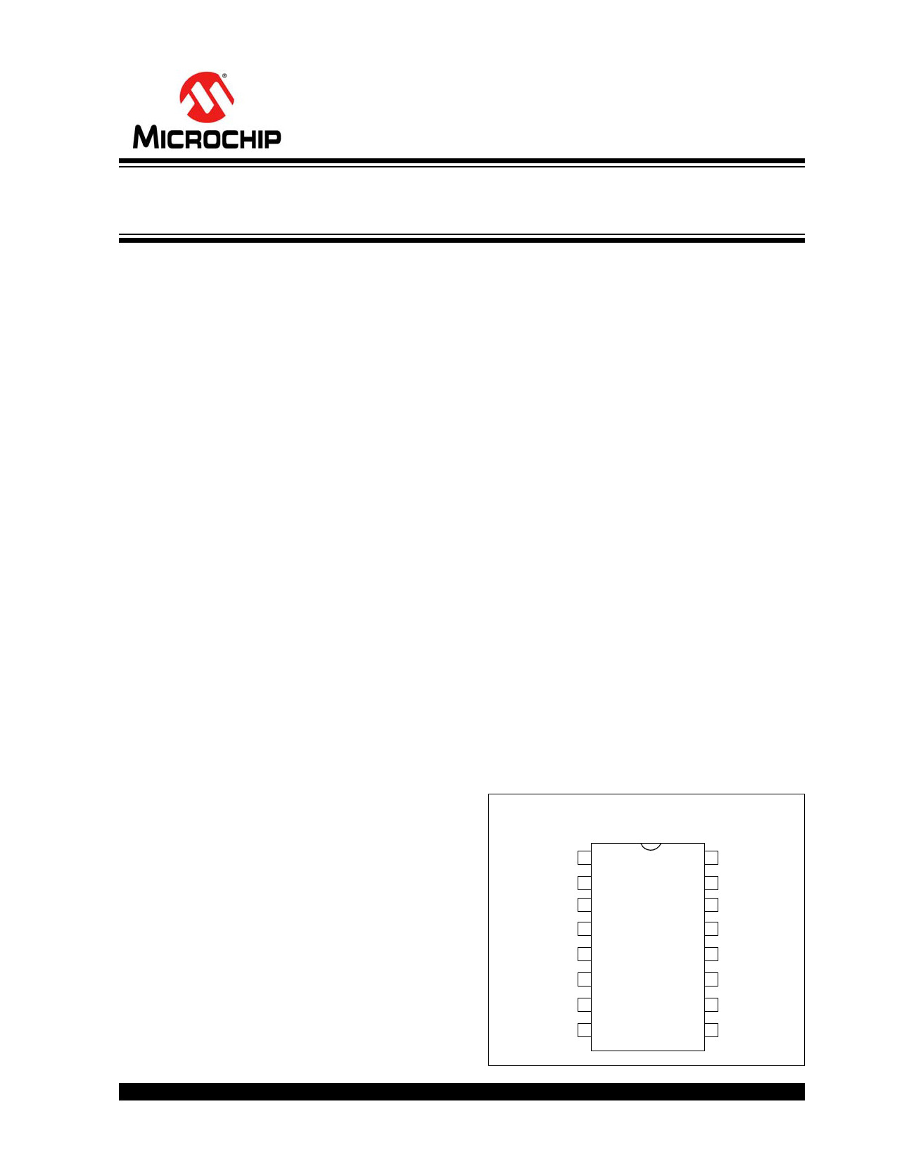
Pin Configuration
C1
1
C2
2
DETECT 3
STROBE
4
VDD 5
IRED 6
IO 7
HORNB
8
16 TEST
15 VSEN
14 VSS
13 ROSC
12 COSC
11 LED
10 FEED
9 HORNS
ABSOLUTE MAXIMUM RATINGS
PARAMETER
SYMBOL
VALUE
UNITS
Supply Voltage
VDD
15
V
Input Voltage Range Except FEED, IO
FEED Input Voltage Range
IO Input Voltage Range
Input Current except FEED
Operating Temperature
Storage Temperature
Vin
Vinfd
Vio1
Iin
TA
TSTG
-.3 to Vdd +.3
V
-10 to +22
V
-.3 to 17
V
10
mA
-25 to 75
°C
-55 to 125
°C
Maximum Junction Temperature
TJ
150
°C
Stresses beyond those listed under Absolute Maximum Ratings may cause permanent damage to the device. These are stress ratings only
and operation at these conditions for extended periods may affect device reliability.
This product utilizes CMOS technology with static protection; however proper ESD prevention procedures should be used when handling this
product. Damage can occur when exposed to extremely high static electrical charge.
© 2009 Microchip Technology Inc.
DS22181B-page 1
Share Link: