RF3145 查看數據表(PDF) - RF Micro Devices
零件编号
产品描述 (功能)
生产厂家
RF3145 Datasheet PDF : 18 Pages
| |||
RF3145
MODE
GSM
EDGE
Dual Mode Operation
RF INPUT
VRAMP
FIXED
Ramp from 0.2V to 1.6V
(GSM Burst Ramp Signal)
Linear ramp from AGC Amplifier/Source (GSM Burst FIXED
Ramp Signal)
TX ENABLE
High (Normal)
Low (Isolation)
High (Normal)
Low (Isolation)
VMODE
Low
High
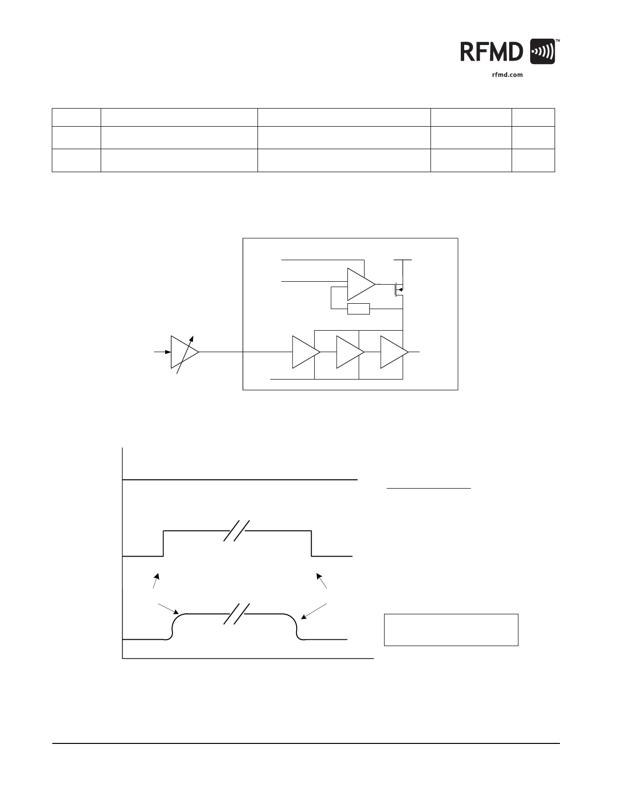
RF3145 Power Amplifier
Simplified Block Diagram of a Single Band
TX ENABLE
VRAMP
VBATT
H(s)
AGC Amplifier
RF IN
TX ENABLE
RF OUT
Power On Sequence
3.0 V to 4.8 V
VBATT
TX_ENABLE
> 1.5 V
Power on Sequence:
Apply VBATT
Apply Band Select
Apply RF drive
Apply TX_Enable & VRAMP in unison
The Power Down sequence is in reverse
order to the Power On Sequence.
VRAMP starts 1us after TX_Enable
0.15 V to 1.6 V
VRAMP
VRAMP settles at 0.2 V 1us before TX_Enable goes low
*NOTE: VBATT must be present
before applying VREG to protect
the ESD circuit from damage.
12 of 18
7628 Thorndike Road, Greensboro, NC 27409-9421 · For sales or technical
support, contact RFMD at (+1) 336-678-5570 or sales-support@rfmd.com.
Rev A4 DS050919
Share Link: 