RF3806 查看數據表(PDF) - RF Micro Devices
零件编号
产品描述 (功能)
生产厂家
RF3806 Datasheet PDF : 18 Pages
| |||
RF3806
PCB Design Requirements
PCB Surface Finish
The PCB surface finish used for RFMD's qualification process is electroless nickel, immersion gold. Typical thickness is 3μinch
3
to 8μinch gold over 180μinch nickel.
PCB Land Pattern Recommendation
PCB land patterns are based on IPC-SM-782 standards when possible. The pad pattern shown has been developed and tested
for optimized assembly at RFMD; however, it may require some modifications to address company specific assembly pro-
cesses. The PCB land pattern has been developed to accommodate lead and package tolerances.
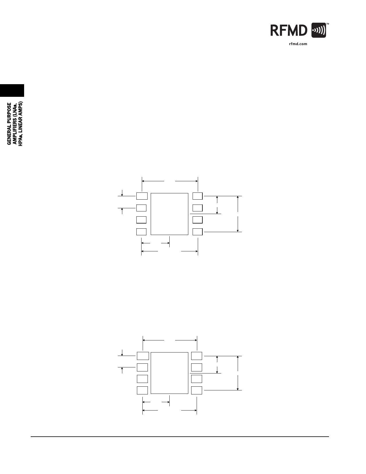
PCB Metal Land Pattern
A = 1.14 x 0.71
B = 1.02 x 0.71 Typ.
C = 3.96 x 4.44
Dimensions in mm.
5.93
Pin 1
A
B
1.27 Typ.
B
B 1.90
C
3.81 Typ.
B
B
B
B
3.00
5.99 Typ.
PCB Solder Mask Pattern
Liquid Photo-Imageable (LPI) solder mask is recommended. The solder mask footprint will match what is shown for the PCB
metal land pattern with a 2mil to 3mil expansion to accommodate solder mask registration clearance around all pads. The
center-grounding pad shall also have a solder mask clearance. Expansion of the pads to create solder mask clearance can be
provided in the master data or requested from the PCB fabrication supplier.
A = 1.30 x 0.86
B = 1.17 x 0.86 Typ.
C = 4.11 x 4.60
Dimensions in mm.
5.93
Pin 1
A
B
1.27 Typ.
B
B
1.90
C
3.81 Typ.
B
B
B
B
3.00
5.99 Typ.
3-130
7628 Thorndike Road, Greensboro, NC 27409-9421 · For sales or technical
support, contact RFMD at (+1) 336-678-5570 or sales-support@rfmd.com.
Rev A3 DS070509
Share Link: 