RT9006A 查看數據表(PDF) - Richtek Technology
零件编号
产品描述 (功能)
生产厂家
RT9006A Datasheet PDF : 10 Pages
| |||
RT9006A/B
Functional Pin Description
Pin No.
Pin Name Pin Function
1
VOUT1 Channel 1 Output Voltage
2
VIN1
Channel 1 Supply Voltage
3
VIN2
Channel 2 Supply Voltage
4
VOUT2 Channel 2 Output Voltage
5
CT
RESET Delay Capacitor
6
R ST
Detect VOUT 2 Output Voltage
7, 8
GND
Common Ground
Exposed Pad (9) GND
The exposed pad must be soldered to a large PCB and connected to
GND for maximum power dissipation.
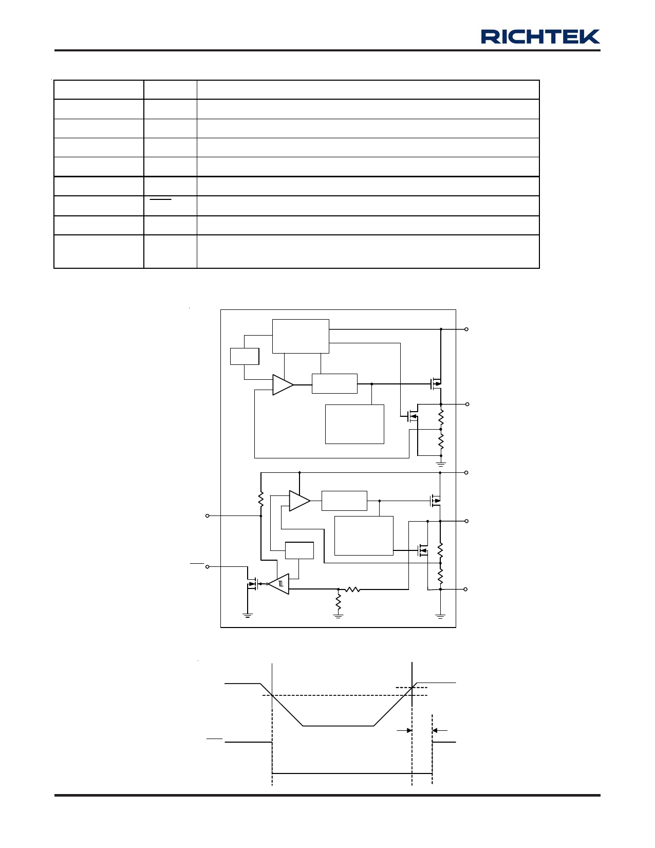
Function Block Diagram
VREF
Shutdown
and
Logic Control
+
-
Error
Amplifier
MOS Driver
Current-Limit
and
Thermal
Protection
VIN1
VOUT1
CT
RST
+
-
Error
Amplifier
VREF
MOS Driver
Current-Limit
and
Thermal
Protection
-
+
VD
Comparator
VIN2
VOUT2
GND
RESET Waveform
3.3V
VOUT2
2.8V
RST
ΔVHYS
Td
www.richtek.com
2
DS9006A/B-05 September 2007
Share Link: 