M80C186 查看數據表(PDF) - Intel
零件编号
产品描述 (功能)
生产厂家
M80C186 Datasheet PDF : 59 Pages
| |||
M80C186
15
14
13 12 11 10 9 8 7 6 5 4 3 2 1 0
OFFSET FEH ET SLAVE MASTER X M IO
Relocation Address Bits R19 – R8
ET e ESC Trap No ESC Trap (1 0)
M IO e Register block located in Memory I O Space (1 0)
SLAVE MASTER e Configures interrupt controller for Slave Master Mode (1 0)
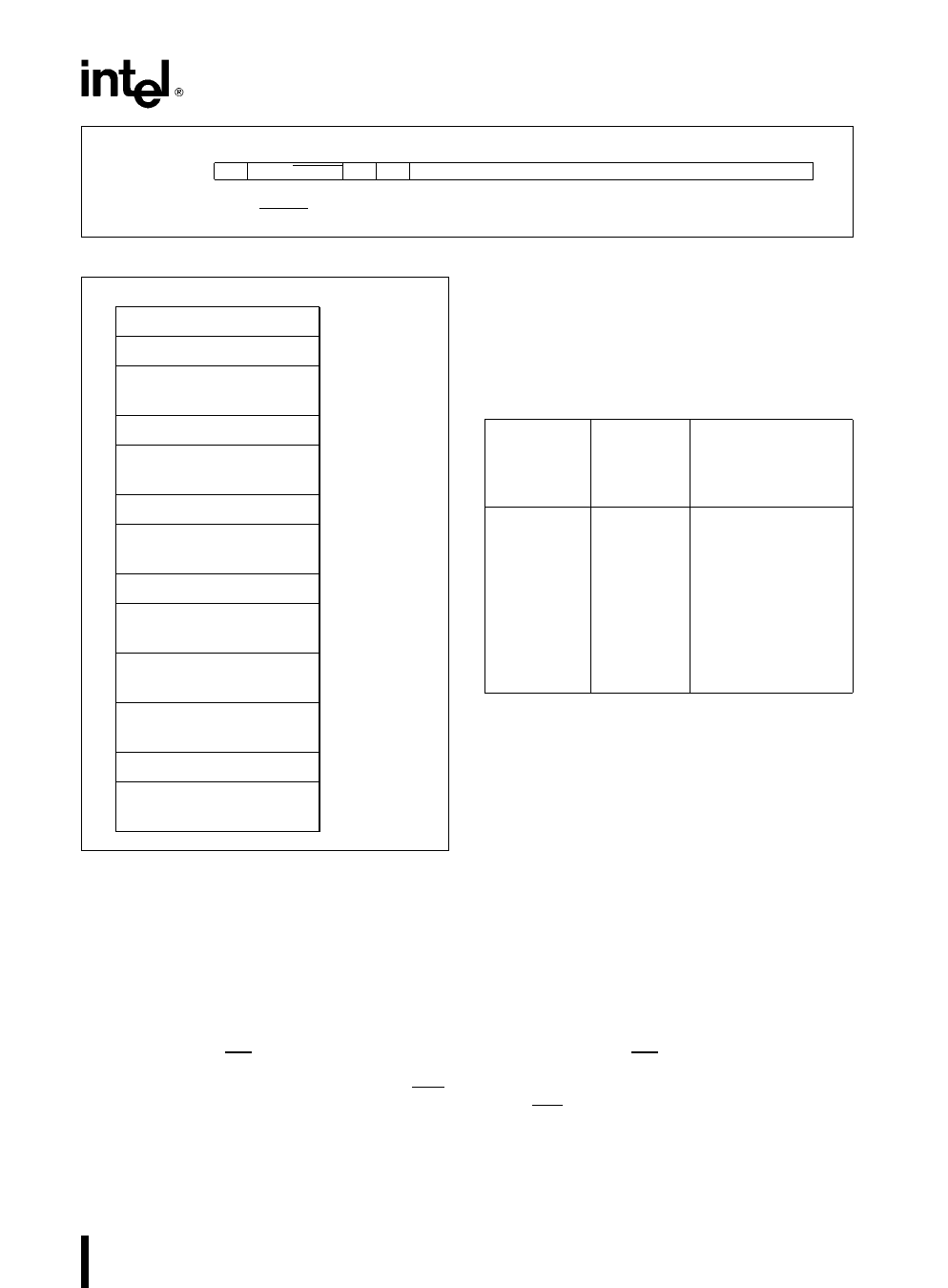
Figure 9 Relocation Register
Relocation Register
OFFSET
FEH
DMA Descriptors Channel 1
DAH
D0H
DMA Descriptors Channel 0
CAH
C0H
A8H
Chip-Select Control Registers
A0H
66H
Time 2 Control Registers
60H
5EH
Time 1 Control Registers
58H
56H
Time 0 Control Registers
50H
3EH
Interrupt Controller Registers
20H
Figure 10 Internal Register Map
of the midrange memory chip select may also be
selected Only one chip select may be programmed
to be active for any memory location at a time
M80C186 memory is arranged in words but chip se-
lects are sized in bytes If sixteen 64K x 1 memories
are used then the memory block size will be 128K
not 64K
The upper limit of memory defined by this chip select
is always FFFFFH while the lower limit is program-
mable By programming the lower limit the size of
the select block is also defined Table 7 shows the
relationship between the base address selected and
the size of the memory block obtained
Table 7 UMCS Programming Values
Starting
Address
(Base
Address)
Memory
Block
Size
UMCS Value
(Assuming
R0eR1eR2e0)
FFC00
FF800
FF000
FE000
FC000
F8000
F0000
E0000
C0000
1K
2K
4K
8K
16K
32K
64K
128K
256K
FFF8H
FFB8H
FF38H
FE38H
FC38H
F838H
F038H
E038H
C038H
The lower limit of this memory block is defined in the
UMCS register (see Figure 11) This register is at
offset A0H in the internal control block The legal
values for bits 6 – 13 and the resulting starting ad-
dress and memory block sizes are given in Table 7
Any combination of bits 6 – 13 not shown in Table 7
will result in undefined operation After reset the
UMCS register is programmed for a 1K area It must
be reprogrammed if a larger upper memory area is
desired
Any internally generated 20-bit address whose up-
per 16 bits are greater than or equal to UMCS (with
bits 0 – 5 ‘‘0’’) will cause UCS to be activated UMCS
bits R2 – R0 are used to specify READY mode for the
area of memory defined by this chip-select register
as explained below
Upper Memory CS
The M80C186 provides a chip select called UCS
for the top of memory The top of memory is usually
used as the system memory because after reset the
M80C186 begins executing at memory location
FFFF0H
Lower Memory CS
The M80C186 provides a chip select for low memory
called LCS The bottom of memory contains the in-
terrupt vector table starting at location 00000H
21
Share Link: 