TDA1314 查看數據表(PDF) - Philips Electronics
零件编号
产品描述 (功能)
生产厂家
TDA1314 Datasheet PDF : 15 Pages
| |||
Philips Semiconductors
Quadruple filter DAC
Product specification
TDA1314T
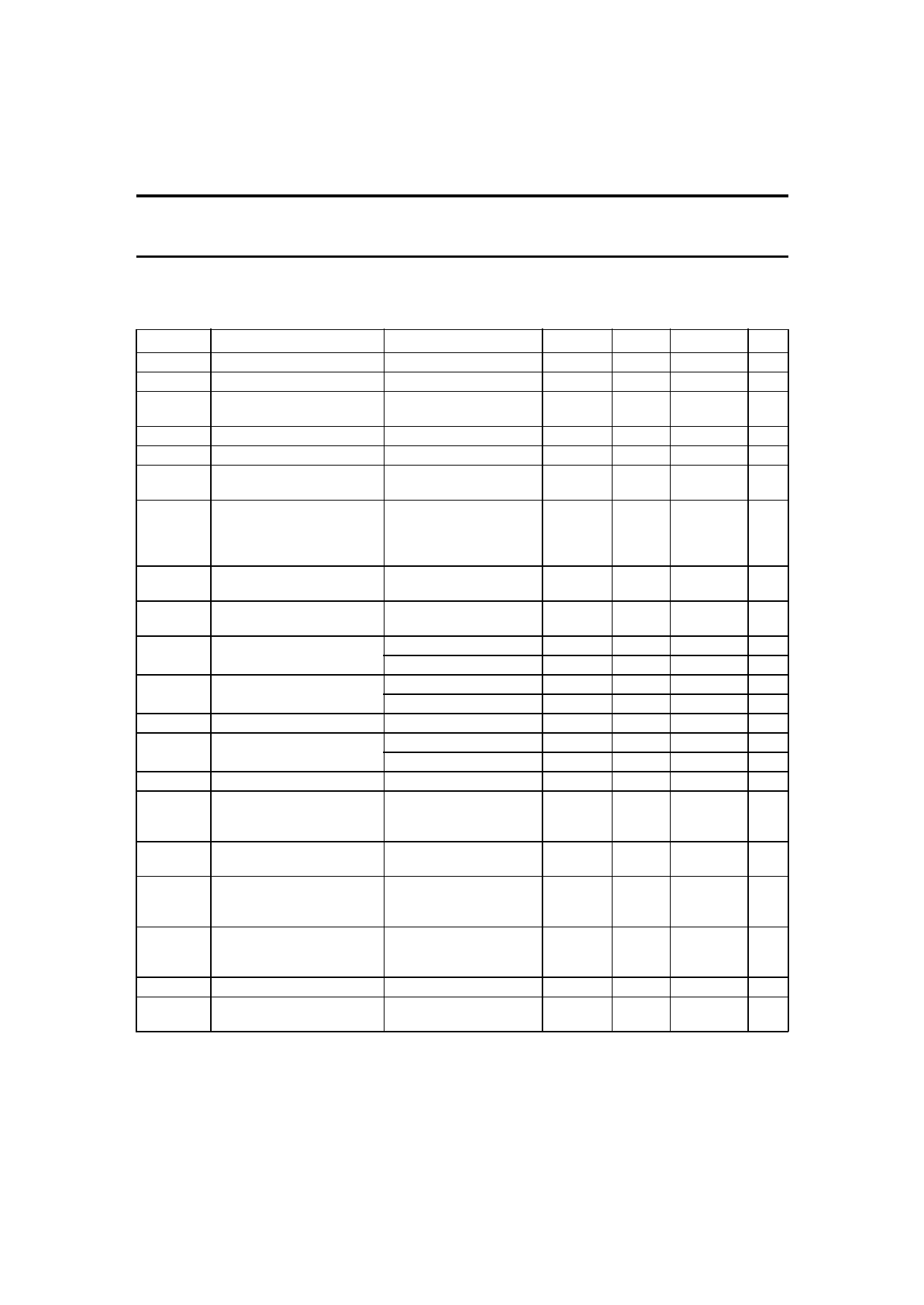
DC CHARACTERISTICS
VDD = 4.5 to 5.5 V; VDDA = VDDO = 4.75 to 5.25 V; all voltage referenced to ground (pins 6, 7 and 15); measured in test
circuit of Fig.6; Tamb = 25 °C; unless otherwise specified.
SYMBOL
PARAMETER
CONDITIONS
MIN.
TYP.
MAX. UNIT
VDDD
VDDA
VDDO
digital supply voltage
analog supply voltage
operational amplifier supply
voltage
4.5
5.0
5.5
V
4.75
5.0
5.25
V
4.75
5.0
5.25
V
IDDD
digital supply current
MCLK = 6.84 MHz
−
10
17
mA
IDDA
analog supply current
at digital silence
−
5
8
mA
IDDO
operational amplifiers supply no operational amplifier −
2
4
mA
current
load resistor
Ptot
total power dissipation
MCLK = 6.84 MHz;
−
at digital silence;
no operational amplifier
load resistor
85
145
mW
VIH
HIGH level input voltage
pins 1 to 5 and 23 to 26
0.7VDDD −
−
V
VIL
LOW level input voltage
pins 1 to 5 and 23 to 26
−
−
0.2VDDD
V
VOH
VOL
Vref
ZI
VI
IODAC(max)
VO(os)
VOH(O)
HIGH level output voltage
pins 27 and 28
LOW level output voltage
pins 27 and 28
reference input voltage
input impedance at pin 21
input voltage pin 14
maximum output current
from DACs pins 10, 12, 17
and 19
DC offset voltage at pins 10,
12, 17 and 19
HIGH level output voltage of
operational amplifiers at
pins 11, 13, 18 and 20
VDDD = 4.5 V; IO = −4 mA 4.1
−
−
V
VDDD = 5.5 V; IO = −4.5 mA 5.1
−
−
V
VDDD = 4.5 V; IO = 4 mA −
−
0.4
V
VDDD = 5.5 V; IO = 4.5 mA −
−
0.4
V
with respect to OGND
0.45VDDO 0.5VDDO 0.55VDDO V
with respect to VDDO
15
20
30
kΩ
with respect to OGND
15
20
30
kΩ
with respect to OGND
0.43VDDO 0.5VDDO 0.57VDDO V
Rref = 20.5 kΩ; VDDO = 5 V 400
500
600
µA
with respect to Vref
note 1; RL > 5 kΩ;
Rfb = 3 kΩ;
maximum signal
−
5
−
mV
VDDO − 1.3 VDDO − 1 VDDO − 0.45 V
VOL(O)
LOW level output voltage of note 1; RL > 5 kΩ;
0.45
1.0
1.3
V
operational amplifiers at
Rfb = 3 kΩ;
pins 11, 13, 18 and 20
maximum signal
Rpu
internal resistance at pin 22 with respect to VDDO
110
160
240
kΩ
Rpd
internal resistance at
Vi = VDDD; with respect to 27
−
80
kΩ
pins 1 to 3 and 23
DGND
Note
1. RL is the AC impedance of the external circuitry connected to the audio outputs in the application diagram of Fig.6.
August 1994
9
Share Link: 