UPD43256B-AXX 查看數據表(PDF) - NEC => Renesas Technology
零件编号
产品描述 (功能)
生产厂家
UPD43256B-AXX Datasheet PDF : 24 Pages
| |||
µPD43256B
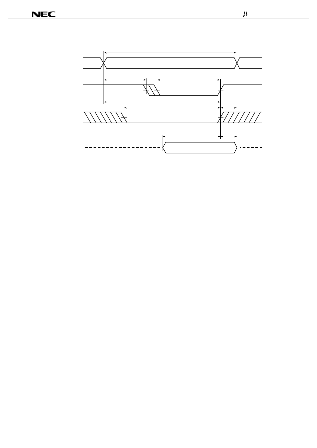
Write Cycle Timing Chart 2 (/CS Controlled)
Address (Input)
/CS (Input)
/WE (Input)
tWC
tAS
tCW
tAW
tWP
tWR
I/O (Input)
High impedance
tDW
Data in
tDH
High
impedance
Cautions 1. /CS or /WE should be fixed to high level during address transition.
•
2. When I/O pins are in the output state, therefore the input signals must not be applied to
the output.
Remark Write operation is done during the overlap time of a low level /CS and a low level /WE.
Data Sheet M10770EJCV0DS00
15
Share Link: 