UPD75236GJ 查看數據表(PDF) - NEC => Renesas Technology
零件编号
产品描述 (功能)
生产厂家
UPD75236GJ Datasheet PDF : 190 Pages
| |||
µPD75236
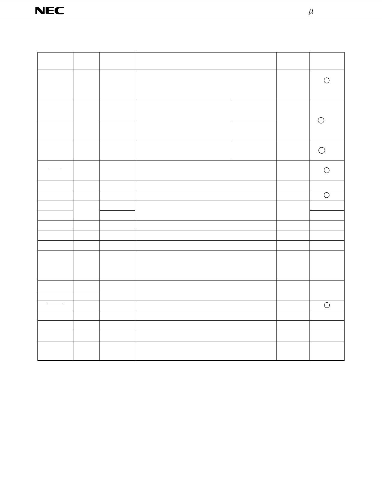
1.2 NON-PORT PINS (2/2)
Pin Name
INT4
I/O
Dual-
Function Pin
Function
Input
P00
Edge-detected vectored interrupt input pin (valid for
detection of rising and falling edges)
After Reset Input / Output
Circuit Type *
—
B
INT0
INT1
Input
P10
Edge-detected vectored interrupt
Clocked
input pin (detected edge selection
P11
possible)
Asynchronous
INT2
Input
SCK1
Input/
output
SO1
SI1
AN0 to AN3
AN4 to AN7
AVDD
AVREF
AVSS
Output
Input
Input
—
Input
—
X1, X2
Input
XT1
XT2
RESET
PP0
VDD (3 – Pin)
VSS (2 – Pin)
Input
—
Input
Output
—
—
VLOAD
—
Edge-detected testable input pin
P12
(rising edge detection)
Asynchronous
P81
Serial clock input/output pin
P82
Serial data output pin
P83
Serial data input pin
—
P90 to P93
—
—
—
Analog input pin to A/D converter
A/D converter power supply pin
A/D converter reference voltage input pin
A/D converter reference GND potential pin
Main system clock oscillation crystal/ceramic connect
—
pin. An external clock is input to X1 and an antiphase
clock is input to X2.
Subsystem clock oscillation crystal connect pin. An
—
external clock is input to XT1 and XT2 is made open.
—
System reset input pin
P80
Timer/pulse generator pulse output pin
—
Positive power supply pin
—
GND potential pin
FIP controller/driver pull-down resistor connect/power
—
supply pin
* Schmitt trigger inputs are circled.
—
—
Input
Input
Input
—
—
—
—
—
—
—
Input
—
—
—
B –C
B –C
F
E
B
Y
Y–A
—
Z
—
—
—
B
—
—
—
—
10
Share Link: 