UPSD3233 查看數據表(PDF) - STMicroelectronics
零件编号
产品描述 (功能)
生产厂家
UPSD3233
STMicroelectronics

UPSD3233 Datasheet PDF : 170 Pages
| |||
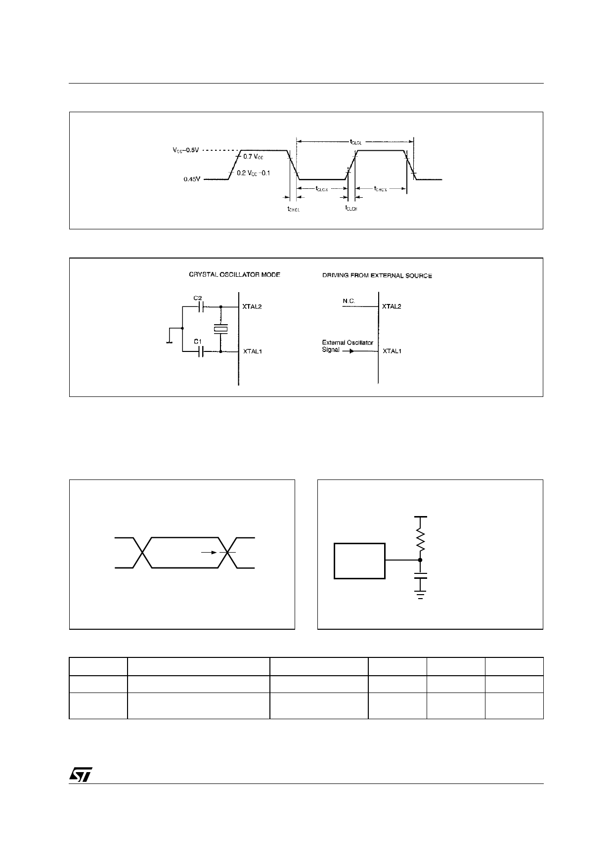
Figure 89. External Clock Cycle
uPSD3234A, uPSD3234BV, uPSD3233B, uPSD3233BV
Figure 90. Recommended Oscillator Circuits
Note: C1, C2 = 30pF ± 10pF for crystals
For ceramic resonators, contact resonator manufacturer
Oscillation circuit is designed to be used either with a ceramic resonator or crystal oscillator. Since each crystal and ceramic resonator
have their own characteristics, the user should consult the crystal manufacturer for appropriate values of external components.
Figure 91. PSD Module AC Measurement I/O
Waveform
Figure 92. PSD ModuleAC Measurement Load
Circuit
3.0V
0V
Test Point
1.5V
AI03103b
Device
Under Test
2.01 V
195 Ω
CL = 30 pF
(Including Scope and
Jig Capacitance)
AI03104b
Table 146. Capacitance
Symbol
Parameter
Test Condition
CIN
COUT
Input Capacitance (for input pins)
Output Capacitance (for input/
output pins)
VIN = 0V
VOUT = 0V
Note: 1. Sampled only, not 100% tested.
2. Typical values are for TA = 25°C and nominal supply voltages.
Typ.2
4
8
Max.
6
12
Unit
pF
pF
163/170
Share Link: