NX25P40-VNI-G 查看數據表(PDF) - Winbond
零件编号
产品描述 (功能)
生产厂家
NX25P40-VNI-G Datasheet PDF : 35 Pages
| |||
W25P10, W25P20 AND W25P40
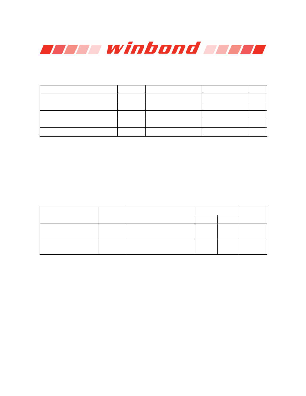
8. ELECTRICAL CHARACTERISTICS
8.1 Absolute Maximum Ratings (1)
PARAMETERS
Supply Voltage
Voltage Applied to Any Pin
Storage Temperature
Lead Temperature
Electrostatic Discharge Voltage
SYMBOL
VCC
VIO
TSTG
TLEAD
VESD
CONDITIONS
Relative to Ground
Human Body Model(3)
RANGE
–0.6 to +4.0
–0.6 to VCC +0.4
–65 to +150
See Note 2
–2000 to +2000
UNIT
V
V
°C
°C
V
Notes:
1 This device has been designed and tested for the specified operation ranges. Proper operation outside of these levels is not
guaranteed. Exposure beyond absolute maximum ratings (listed above) may cause permanent damage.
2. Compliant with JEDEC Standard J-STD-20C for small body Sn-Pb or Pb-free (Green) assembly and the European directive
on restrictions on hazardous substances (RoHS) 2002/95/EU..
3. JEDEC Std JESD22-A114A (C1=100 pF, R1=1500 ohms, R2=500 ohms).
8.2 Operating Ranges
PARAMETER
SYMBOL CONDITIONS
Supply Voltage(1)
VCC
Ambient Temperature, TA
Operating
FR = 33MHz, fR = 25MHz
FR = 40MHz, fR = 25MHz
Industrial
SPEC
MIN
MAX
2.7
3.6
3.0
3.6
–40
+85
UNIT
V
V
°C
Note:
1. VCC voltage during Read can operate across the min and max range but should not exceed ±10% of the programming
(erase/write) voltage.
Publication Release Date: November 28, 2005
- 25 -
Revision M
Share Link: 