L9949 查看數據表(PDF) - STMicroelectronics
零件编号
产品描述 (功能)
生产厂家
L9949 Datasheet PDF : 20 Pages
| |||
L9949
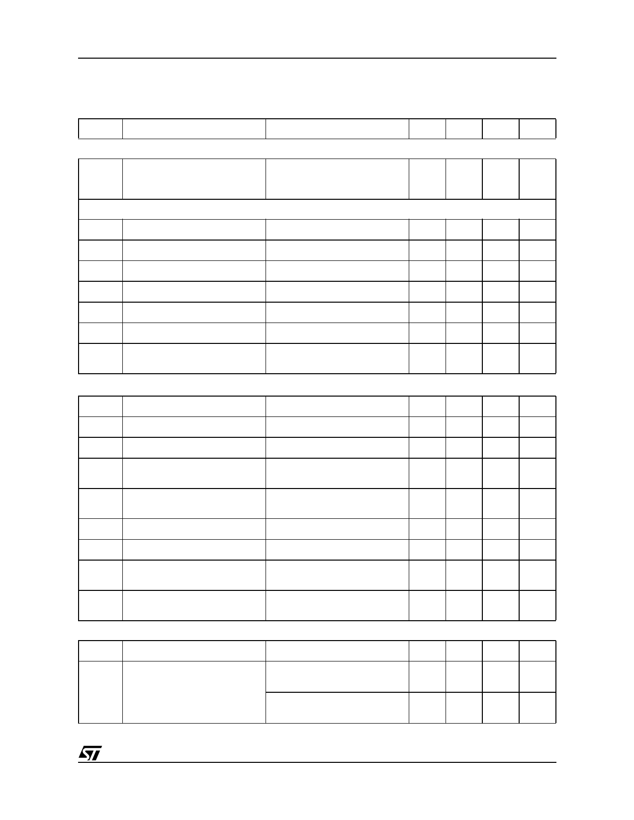
SPI INTERFACE ELECTRICAL CHARACTERISTCS
VS = 8 to 16 V, VCC = 4.5 to 5.5 V, Tj = -40 to 150 °C, unless otherwise specified. The voltages are refered to
GND and currents are assumed positive, when the current flows into the pin.
Symbol
Parameter
Test Condition
Min. Typ. Max. Unit
Delay time from standby to active mode
tset Delay Time
Switching from standby to active
mode. Time until output drivers are
enabled after CSN going to high.
200
µs
Inputs: CSN, CLK and DI
VINL Input Low Level
VCC = 5 V
1.5
V
VINH Input High Level
VCC = 5 V
3.5
V
VINHyst Input Hystersis
VCC = 5 V
0.5
V
ICSNin Pull Up Current at input CSN
VCSN = 3.5 V
-50
-25
-10
µA
ICLK in Pull Down Current at input CLK VCLK = 1.5 V
10
25
50
µA
IDI in Pull Down Current at input DI
VDI = 1.5 V
10
25
50
µA
Cin(1) Input Capacitance at input CSN 0 V < VCC < 5.5 V
or CLK
10
15
pF
DI timing (see Fig. 9 )(2)
tCLK Clock Period
VCC = 5 V
1000
ns
tCLKH Clock High Time
VCC = 5 V
400
ns
tCLKL Clock Low Time
VCC = 5 V
400
ns
tset CSN CSN setup time, CSN low before VCC = 5 V
rising edge of CLK
400
ns
tset CLK CLK setup time, CLK high before VCC = 5 V
rising edge of CSN
400
ns
tset DI DI setup time
VCC = 5 V
200
ns
thold DI DI hold time
VCC = 5 V
200
ns
tr-in Rise Time of Input Signal
DI, CLK, CSN
VCC = 5 V
100
ns
tf-in Fall Time of Input Signal
DI, CLK, CSN
VCC = 5 V
100
ns
DO
VDOL Output Low Level
VCC = 5 V, ID = -4 mA
0.2
0.4
V
VDOH Output High Level
VCC = 5 V, ID = -4 mA
VCC
VCC
V
-1.3 -1.0
VCC = 5 V, ID = -200 µA; Tj = 25°C VCC
V
-0.8
15/20
Share Link: 