MCP6N16T-100 查看數據表(PDF) - Microchip Technology
零件编号
产品描述 (功能)
生产厂家
MCP6N16T-100 Datasheet PDF : 58 Pages
| |||
MCP6N16
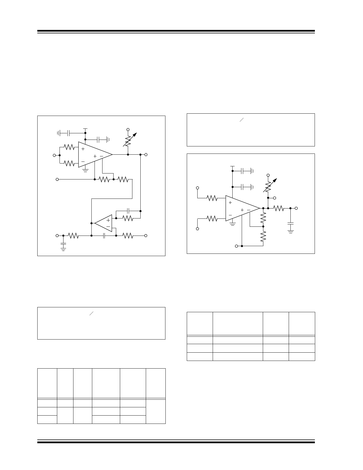
1.4 DC Test Circuits
1.4.1 INPUT OFFSET TEST CIRCUIT
Figure 1-7 is a simple circuit that can test the INA’s
input offset errors and input voltage range (VE, VIVL and
VIVH; see Section 1.5.1 “Input Offset Related
Errors” and Section 1.5.2 “Input Offset Common
Mode Nonlinearity”). U2 is part of a control loop that
forces VOUT to equal VCNT; U1 can be set to any bias
point.
VCM
VREF
VDD
2.2 µF
100 nF
VL
RL
100Ω
100Ω
U1
MCP6N16
RG
RF
100Ω
VOUT
U2
MCP6H01
31.6 kΩ
VM
10 µF
2.2 nF
31.6 kΩ
CCNT
RCNT
2.2 nF 31.6 kΩ
VCNT
FIGURE 1-7:
Simple Test Circuit for
Common Mode (Input Offset).
When MCP6N16 is in its normal range of operation, the
DC output voltages are (where VE is the sum of input
offset errors and gE is the gain error):
EQUATION 1-1:
GDM = 1 + RF RG
VOUT = VCNT
VM = VREF + GDM1 + gEVE
Table 1-5 shows the resulting behavior for different
GMIN options.
TABLE 1-5: RESULTS
GMIN RF GDM GDMVOS
(V/V) (kΩ) (kV/V) (±mV)
Nom. Typ. Typ. Max.
1 100 1.00
85
10 402 4.02
88
100
68
BW
(kHz)
Typ.
at VOUT
0.50
1.2
8.7
BW
(Hz)
Typ.
at VM
0.50
1.4.2 DIFFERENTIAL GAIN TEST CIRCUIT
Figure 1-8 is a simple circuit that can test the INA’s
differential gain error, nonlinearity and input voltage
range (gE, INLDM, VDML and VDMH; see Section 1.5.3
“Differential Gain Error and Nonlinearity”). RF and
RG are 0.01% for accurate gain error measurements.
The output voltages are (where VE is the sum of input
offset errors and gE is the gain error):
EQUATION 1-2:
GDM = 1 + RF RG
VOUT = VREF + GDM1 + gEVDM + VE
VM = VREF + GDM1 + gEVDM + VE
VDD
VL
VCM + VDM/2 2.2 µF
100Ω
U1
MCP6N16
100 nF
RF
RL
VOUT
63.4 kΩ
VM
100Ω
1.0 µF
VCM – VDM/2
RG
VREF
FIGURE 1-8:
Simple Test Circuit for
Differential Mode.
For different values of VREF, VDM sweeps over different
ranges to keep VREF, VFG and VOUT within their ranges.
Table 1-6 shows the recommended RF and RG; they
produce a 10 kΩ load. VL can usually be left open.
TABLE 1-6:
GMIN
(V/V)
Nom.
SELECTING RF AND RG
RF
(kΩ)
Nom.
RG
(kΩ)
Nom.
GDM
(V/V)
Nom.
1
0
Open 1.0000
10
10.0 || 90.9
1.00 10.009
100
10.0 || 1000
100
100.01
1.4.3
DYNAMIC TESTING OF INPUT
BEHAVIOR
The circuit in Figure 1-8 can test the input’s dynamic
behavior (i.e., IMD, tSTR, tSTL, tIRC, tIRD and tOR);
measure the output at VOUT, instead of at VM.
DS20005318A-page 14
2014 Microchip Technology Inc.
Share Link: 