MCP6N16-001E/MF 查看數據表(PDF) - Microchip Technology
零件编号
产品描述 (功能)
生产厂家
MCP6N16-001E/MF Datasheet PDF : 58 Pages
| |||
MCP6N16
2.0 TYPICAL PERFORMANCE CURVES
Note:
The graphs and tables provided following this note are a statistical summary based on a limited number of
samples and are provided for informational purposes only. The performance characteristics listed herein
are not tested or guaranteed. In some graphs or tables, the data presented may be outside the specified
operating range (e.g., outside specified power supply range) and therefore outside the warranted range.
Note: Unless otherwise indicated, TA = +25°C, VDD = 1.8V to 5.5V, VSS = GND, VCM = VDD/2, VDM = 0V,
VREF = VDD/2, VL = VDD/2, RL = 10 kΩ to VL, CL = 60 pF, GDM = GMIN and EN = VDD; see Figures 1-7 and 1-8.
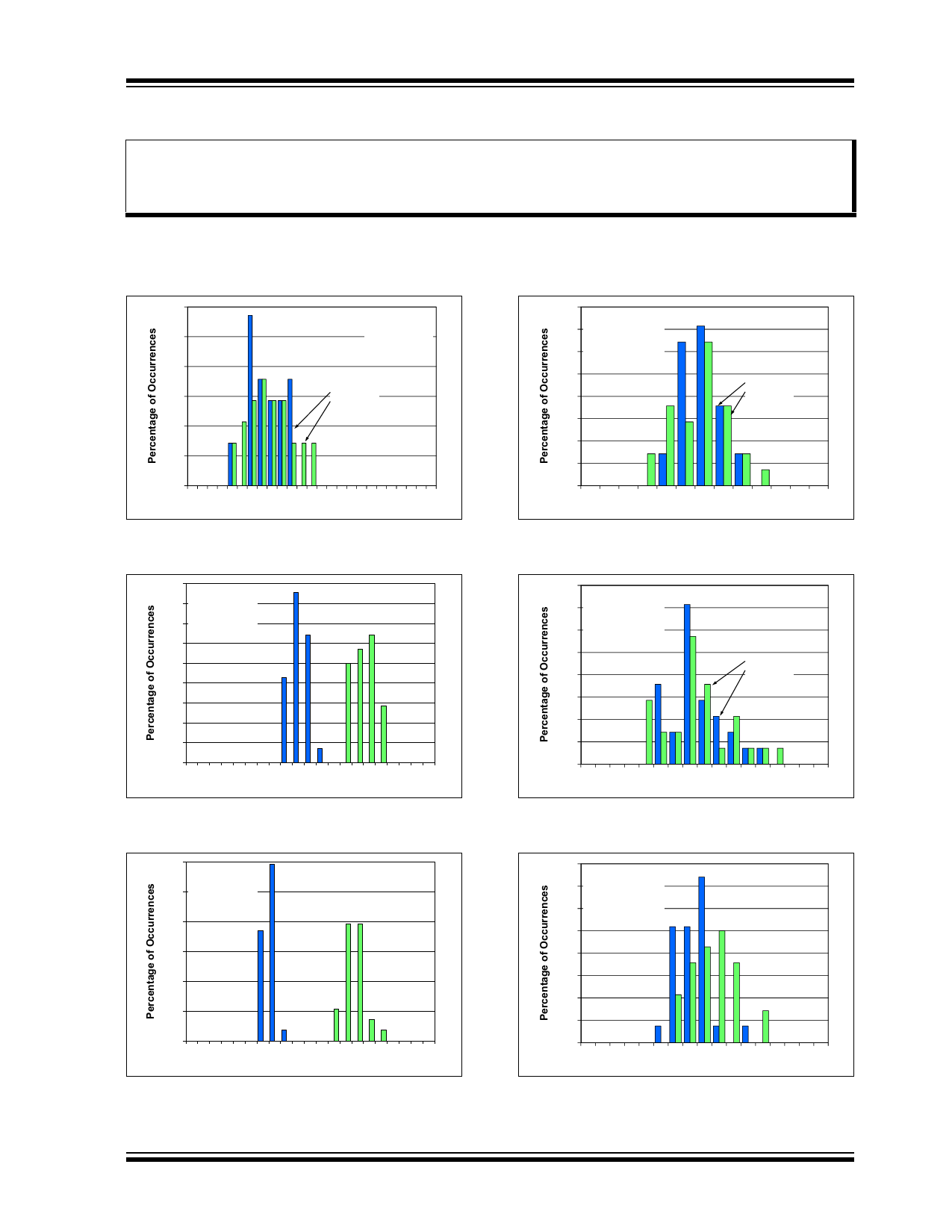
2.1 DC Precision
30%
25%
20%
15%
10%
GMIN = 1
28 Samples
TA = +25°C
NPBW = 3 mHz
VDD = 1.8V
VDD = 5.5V
5%
0%
-12 -10 -8 -6 -4 -2 0 2 4 6 8 10 12
Input Offset Voltage (µV)
FIGURE 2-1:
Input Offset Voltage, with
GMIN = 1.
40%
35%
30%
GMIN = 1
28 Samples
TA = -40 to +125°C
NPBW = 3 mHz
25%
20%
VDD = 1.8V
VDD = 5.5V
15%
10%
5%
0%
-600 -400 -200 0 200 400 600
Input Offset Voltage Drift; TC1 (nV/°C)
FIGURE 2-4:
Input Offset Voltage Drift,
with GMIN = 1.
45%
40%
35%
GMIN = 10
28 Samples
TA = +25°C
NPBW = 3 mHz
30%
25%
20%
15%
VDD = 1.8V
VDD = 5.5V
10%
5%
0%
-2.0 -1.6 -1.2 -0.8 -0.4 0.0 0.4 0.8 1.2 1.6 2.0
Input Offset Voltage (µV)
FIGURE 2-2:
GMIN = 10.
Input Offset Voltage, with
40%
35%
30%
GMIN = 10
28 Samples
TA = -40 to +125°C
NPBW = 3 mHz
25%
20%
VDD = 5.5V
VDD = 1.8V
15%
10%
5%
0%
-40 -30 -20 -10 0 10 20 30 40
Input Offset Voltage Drift; TC1 (nV/°C)
FIGURE 2-5:
Input Offset Voltage Drift,
with GMIN = 10.
60%
50%
40%
GMIN = 100
28 Samples
TA = +25°C
NPBW = 3 mHz
30%
20%
VDD = 1.8V
VDD = 5.5V
10%
0%
-1.0 -0.6 -0.2 0.2 0.6 1.0 1.4 1.8 2.2 2.6 3.0
Input Offset Voltage (µV)
FIGURE 2-3:
GMIN = 100.
Input Offset Voltage, with
40%
35%
30%
GMIN = 100
28 Samples
TA = -40 to +125°C
NPBW = 3 mHz
25%
20%
15%
VDD = 1.8V
VDD = 5.5V
10%
5%
0%
-16 -12 -8 -4 0 4 8 12 16
Input Offset Voltage Drift; TC1 (nV/°C)
FIGURE 2-6:
Input Offset Voltage Drift,
with GMIN = 100.
2014 Microchip Technology Inc.
DS20005318A-page 17
Share Link: 