MCP6N16T-001E 查看數據表(PDF) - Microchip Technology
零件编号
产品描述 (功能)
生产厂家
MCP6N16T-001E Datasheet PDF : 58 Pages
| |||
MCP6N16
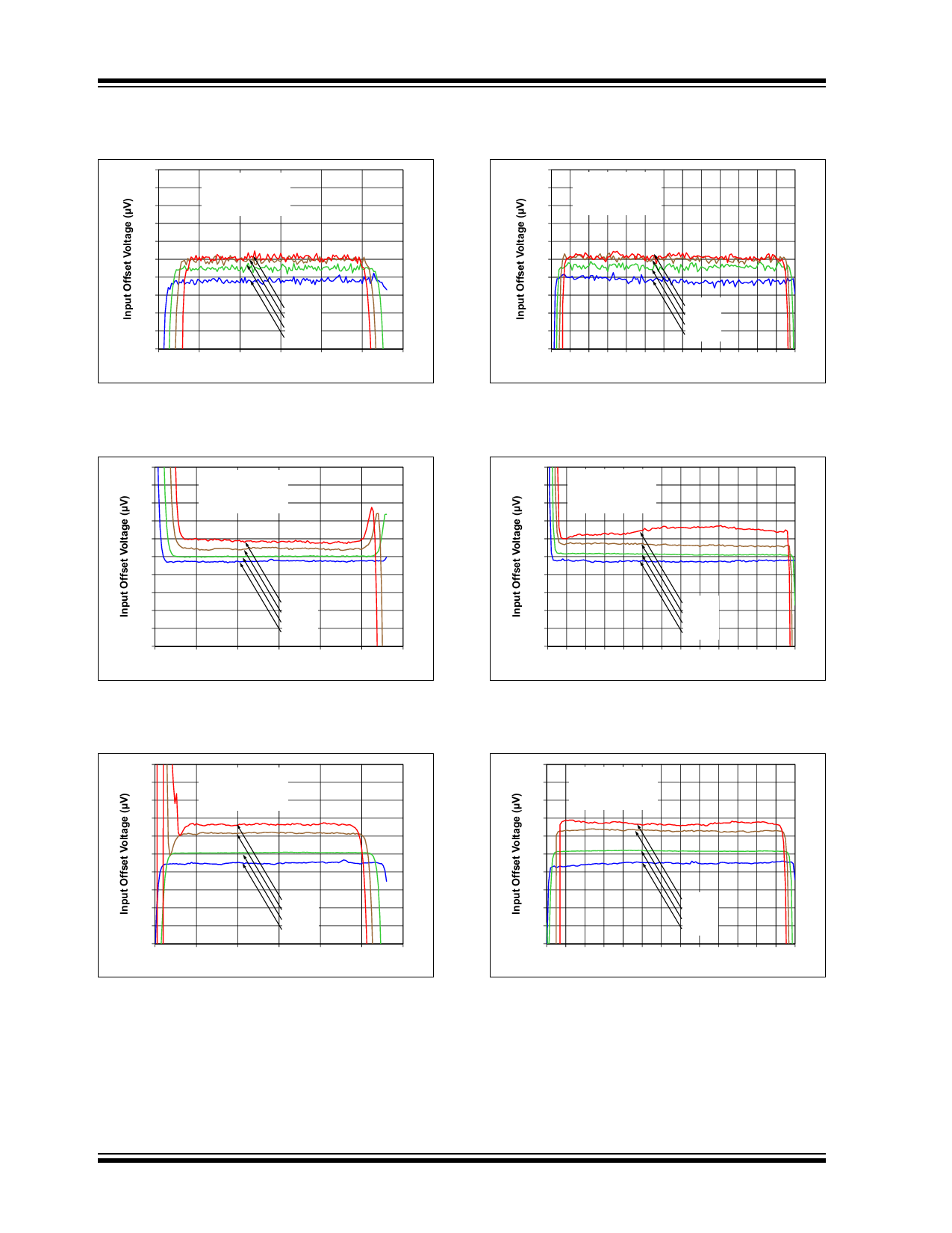
Note: Unless otherwise indicated, TA = +25°C, VDD = 1.8V to 5.5V, VSS = GND, VCM = VDD/2, VDM = 0V,
VREF = VDD/2, VL = VDD/2, RL = 10 kΩ to VL, CL = 60 pF, GDM = GMIN and EN = VDD; see Figures 1-7 and 1-8.
50
Representative Part
40
VDD = 1.8V
30
GMIN = 1
NPBW = 2 Hz
20
10
0
-10
-20
-30
+125°C
+85°C
-40
+25°C
-40°C
-50
-0.5 0.0 0.5 1.0 1.5 2.0 2.5
Input Common Mode Voltage (V)
FIGURE 2-19:
Input Offset Voltage vs.
Common Mode Voltage, with VDD = 1.8V and
GMIN = 1.
50
Representative Part
40
VDD = 5.5V
30
GMIN = 1
NPBW = 2 Hz
20
10
0
-10
-20
+125°C
-30
+85°C
-40
+25°C
-40°C
-50
-0.5 0.0 0.5 1.0 1.5 2.0 2.5 3.0 3.5 4.0 4.5 5.0 5.5 6.0
Input Common Mode Voltage (V)
FIGURE 2-22:
Input Offset Voltage vs.
Common Mode Voltage, with VDD = 5.5V and
GMIN = 1.
50
Representative Part
40
VDD = 1.8V
30
GMIN = 10
NPBW = 2 Hz
20
10
0
-10
-20
+125°C
-30
+85°C
-40
+25°C
-40°C
-50
-0.5 0.0
0.5
1.0
1.5
2.0
2.5
Input Common Mode Voltage (V)
FIGURE 2-20:
Input Offset Voltage vs.
Common Mode Voltage, with VDD = 1.8V and
GMIN = 10.
50
Representative Part
40
VDD = 5.5V
30
GMIN = 10
NPBW = 2 Hz
20
10
0
-10
-20
+125°C
-30
+85°C
-40
+25°C
-40°C
-50
-0.5 0.0 0.5 1.0 1.5 2.0 2.5 3.0 3.5 4.0 4.5 5.0 5.5 6.0
Input Common Mode Voltage (V)
FIGURE 2-23:
Input Offset Voltage vs.
Common Mode Voltage, with VDD = 5.5V and
GMIN = 10.
50
Representative Part
40
VDD = 1.8V
30
GMIN = 100
NPBW = 2 Hz
20
10
0
-10
-20
+125°C
-30
+85°C
-40
+25°C
-40°C
-50
-0.5 0.0
0.5
1.0
1.5
2.0
2.5
Input Common Mode Voltage (V)
FIGURE 2-21:
Input Offset Voltage vs.
Common Mode Voltage, with VDD = 1.8V and
GMIN = 100.
50
Representative Part
40
VDD = 5.5V
30
GMIN = 100
NPBW = 2 Hz
20
10
0
-10
-20
+125°C
-30
+85°C
+25°C
-40
-40°C
-50
-0.5 0.0 0.5 1.0 1.5 2.0 2.5 3.0 3.5 4.0 4.5 5.0 5.5 6.0
Input Common Mode Voltage (V)
FIGURE 2-24:
Input Offset Voltage vs.
Common Mode Voltage, with VDD = 5.5V and
GMIN = 100.
DS20005318A-page 20
2014 Microchip Technology Inc.
Share Link: 