MCP6N16-001E 查看數據表(PDF) - Microchip Technology
零件编号
产品描述 (功能)
生产厂家
MCP6N16-001E Datasheet PDF : 58 Pages
| |||
In some applications, it may be necessary to prevent
excessive voltages from reaching the INA inputs.
Figure 4-8 shows one approach to protecting these
inputs. D1 and D2 may be small signal silicon diodes,
Schottky diodes for lower clamping voltages or
diode-connected FETs for low leakage.
D1
V1
D2
V2
VDD
U1
MCP6N16
FIGURE 4-8:
Protecting the Analog Inputs
Against High Voltages.
4.3.1.3 Input Current Limits
In order to prevent damage and/or improper operation
of these amplifiers, the circuit must limit the currents
into the input pins (see Section 1.1 “Absolute
Maximum Ratings †”). This requirement is
independent of the voltage limits previously discussed.
Figure 4-9 shows one approach to protecting these
inputs. The resistors R1 and R2 limit the possible
current in or out of the input pins (and into D1 and D2).
The diode currents will dump onto VDD.
VDD
D1
V1
R1 D2
V2
R2
U1
MCP6N16
min(R1,
R2)
>
VSS
–
min(V1,
2 mA
V2)
min(R1, R2) >
max(V1, V2) – VDD
2 mA
FIGURE 4-9:
Protecting the Analog Inputs
Against High Currents.
It is also possible to connect the diodes to the left of the
resistor R1 and R2. In this case, the currents through
the diodes D1 and D2 need to be limited by some other
mechanism. The resistors then serve as in-rush current
limiters; the DC current into the input pins (VIP and VIM)
should be very small.
A significant amount of current can flow out of the
inputs (through the ESD diodes) when the common
mode voltage (VCM) is below ground (VSS); see
Figure 2-47.
MCP6N16
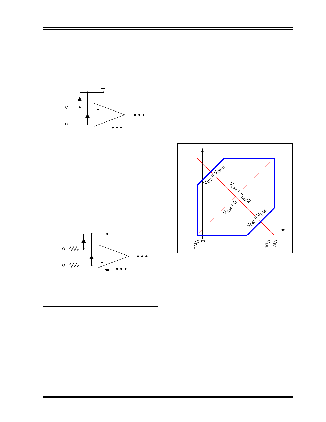
4.3.1.4 Input Voltage Ranges
Figure 4-10 shows possible input voltage values
(VSS = 0V). Lines with a slope of +1 have constant VDM
(e.g., the VDM = 0 line). Lines with a slope of -1 have
constant VCM (e.g., the VCM = VDD/2 line).
For normal operation, VIP and VIM must be kept within
the region surrounded by the thick blue lines. The
horizontal and vertical blue lines show the limits on the
individual inputs. The blue lines with a slope of +1 show
the limits on VDM; the larger GMIN is, the closer they are
to the VDM = 0 line.
The input voltage range specifications (VIVL and VIVH)
change with the supply voltages (VSS and VDD,
respectively). The differential input range specifications
(VDML and VDMH) change with minimum gain (GMIN).
Temperature also affects these specifications.
VIP
VIVH
VDD
0
VIVL
= V DMH
V DM
V
CM = V
= 0 DD /2
V DM
= V DML
V DM
VIM
FIGURE 4-10:
Input Voltage Ranges.
To take full advantage of VDML and VDMH, set VREF
(see Figures 1-7 and 1-8) so that the output (VOUT) is
centered between the supplies (VSS and VDD). Also set
the gain (GDM) to keep VOUT within its range.
2014 Microchip Technology Inc.
DS20005318A-page 41
Share Link: 