MCP6N16-001 查看數據表(PDF) - Microchip Technology
零件编号
产品描述 (功能)
生产厂家
MCP6N16-001 Datasheet PDF : 58 Pages
| |||
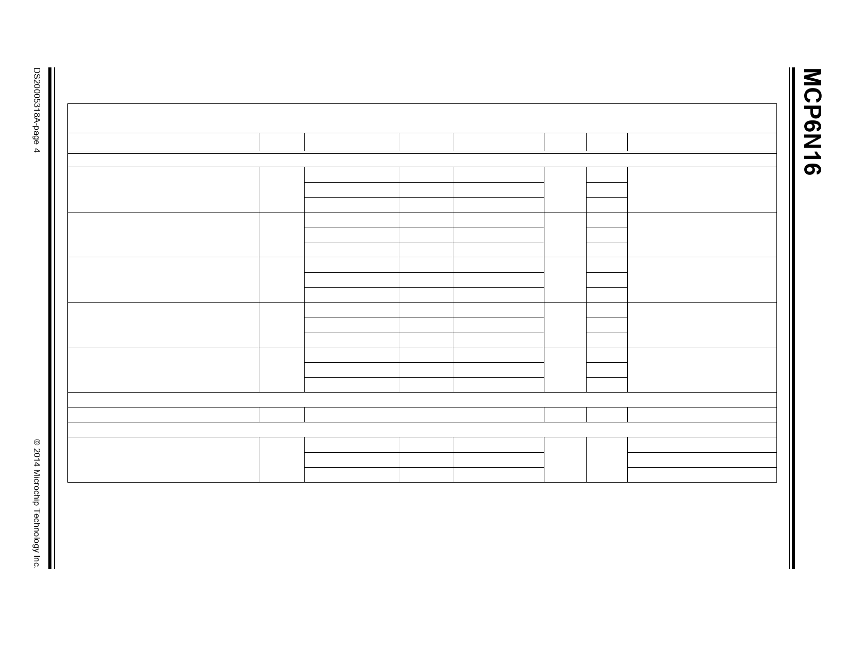
1.2 Specifications
TABLE 1-1: DC ELECTRICAL SPECIFICATIONS
Electrical Characteristics: Unless otherwise indicated, TA = +25°C, VDD = 1.8V to 5.5V, VSS = GND, VCM = VDD/2, VDM = 0V, VREF = VDD/2, VL = VDD/2, RL = 10 kΩ
to VL, GDM = GMIN and EN = VDD; see Figures 1-7 and 1-8 (Note 1).
Parameters
Sym.
Min.
Typ.
Max.
Units GMIN
Conditions
Input Offset
Input Offset Voltage
VOS
-85
-22
—
+85
µV
1 TA = +25°C
—
+22
10
-17
—
+17
100
Input Offset Voltage Drift –
Linear Temp. Co.
TC1
-1800
-180
—
+1800
nV/°C
1 TA = -40°C to +125°C (Note 2)
—
+180
10
Input Offset Voltage Drift –
Quadratic Temp. Co.
-60
TC2
—
—
—
±560
±63
+60
100
—
pV/°C2
1 TA = -40°C to +125°C
—
10
—
±69
—
100
Input Offset Aging
∆VOS
—
—
±1.0
±0.8
—
µV
1 408 hr Life Test at +150°C,
—
10 measured at +25°C
—
±0.7
—
100
Power Supply Rejection Ratio
PSRR
91
109
—
dB
1
104
122
—
10
110
128
—
100
Output Offset
Output Offset Voltage
VOSO
0
Input Current and Impedance (Note 3)
µV
all
Input Bias Current
Across Temperature
IB
-100
—
±2
+100
pA
all
20
—
Across Temperature
0
250
2000
Note 1:
2:
3:
4:
5:
6:
VCM = (VIP + VIM)/2, VDM = (VIP – VIM) and GDM = 1 + RF/RG.
For Design Guidance only; not tested.
These specifications apply to the VIP, VIM input pair (use VCM) and to the VREF, VFG input pair (use VREF instead).
This specification applies to the VIP, VIM, VREF and VFG pins individually.
Figures 2-52 and 2-53 show the VIVL, VIVH, VDML and VDMH variation over temperature.
See Section 1.5 “Explanation of DC Error Specifications”.
TA = +85°C
TA = +125°C
Share Link: 