1N5908 查看數據表(PDF) - ON Semiconductor
零件编号
产品描述 (功能)
生产厂家
1N5908 Datasheet PDF : 6 Pages
| |||
1N5908
MAXIMUM RATINGS
Rating
Symbol
Value
Unit
Peak Power Dissipation (Note 1)
@ TL ≤ 25°C
PPK
1500
W
Steady State Power Dissipation
@ TL ≤ 75°C, Lead Length = 3/8″
Derated above TL = 75°C
Thermal Resistance, Junction−to−Lead
Forward Surge Current (Note 2)
@ TA = 25°C
PD
RqJL
IFSM
5.0
W
50
mW/°C
20
°C/W
200
A
Operating and Storage
Temperature Range
TJ, Tstg
− 65 to +175
°C
Maximum ratings are those values beyond which device damage can occur. Maximum ratings applied to the device are individual stress limit
values (not normal operating conditions) and are not valid simultaneously. If these limits are exceeded, device functional operation is not implied,
damage may occur and reliability may be affected.
1. Nonrepetitive current pulse per Figure 4 and derated above TA = 25°C per Figure 2.
2. 1/2 sine wave (or equivalent square wave), PW = 8.3 ms, duty cycle = 4 pulses per minute maximum.
*Bidirectional device will not be available in this device
ELECTRICAL CHARACTERISTICS (TA = 25°C unless
otherwise noted, VF = 3.5 V Max. @ IF (Note 3) = 100 A)
Symbol
Parameter
IPP
VC
VRWM
IR
VBR
IT
IF
VF
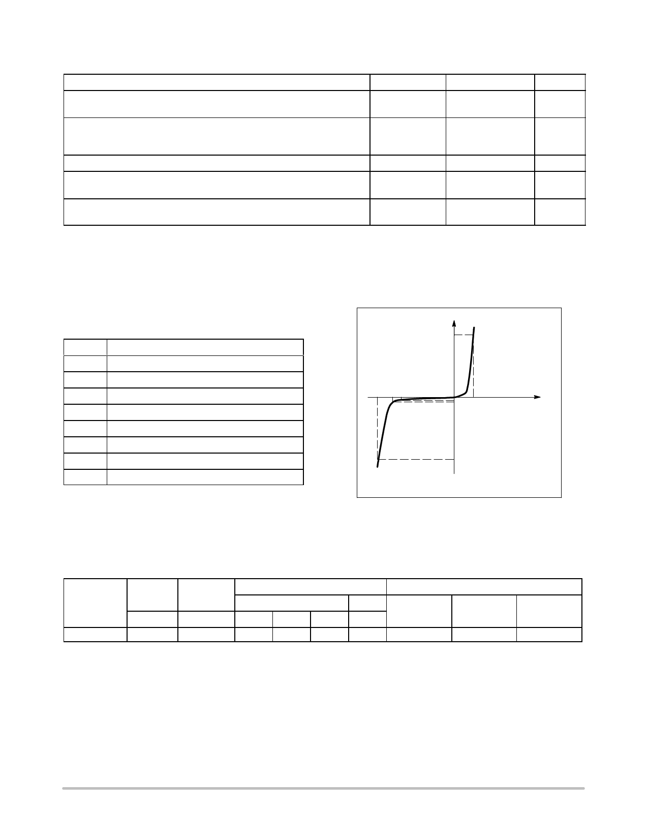
Maximum Reverse Peak Pulse Current
Clamping Voltage @ IPP
Working Peak Reverse Voltage
Maximum Reverse Leakage Current @ VRWM
Breakdown Voltage @ IT
Test Current
Forward Current
Forward Voltage @ IF
I
IF
VC VBR VRWM
IIRT VF
V
IPP
Uni−Directional TVS
ELECTRICAL CHARACTERISTICS (TA = 25°C unless otherwise noted, VF = 3.5 V Max. @ IF (Note 3) = 53 A)
Device
(Note 4)
VRWM
(Note 5)
(Volts)
IR @ VRWM
(mA)
Breakdown Voltage
VBR (Note 6) (Volts)
Min Nom Max
@ IT
(mA)
VC (Volts) (Note 7)
@ IPP = 120 A @ IPP = 60 A @ IPP = 30 A
1N5908
5.0
300
6.0
−
−
1.0
8.5
8.0
7.6
3. Square waveform, PW = 8.3 ms, Non−repetitive duty cycle.
4. 1N5908 is JEDEC registered as a unidirectional device only (no bidirectional option)
5. A transient suppressor is normally selected according to the maximum working peak reverse voltage (VRWM), which should be equal to or
greater than the dc or continuous peak operating voltage level.
6. VBR measured at pulse test current IT at an ambient temperature of 25°C and minimum voltages in VBR are to be controlled.
7. Surge current waveform per Figure 4 and derate per Figure 2 of the General Data − 1500 W at the beginning of this group
http://onsemi.com
2
Share Link: 