1N5908 查看數據表(PDF) - ON Semiconductor
零件编号
产品描述 (功能)
生产厂家
1N5908 Datasheet PDF : 6 Pages
| |||
1N5908
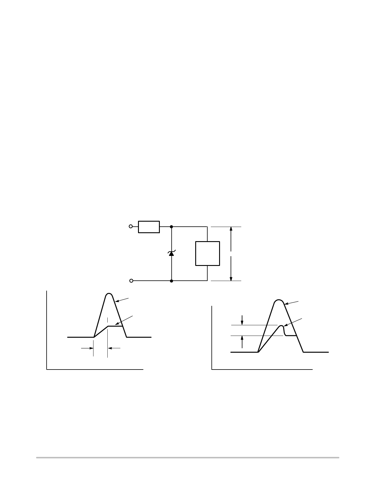
APPLICATION NOTES
RESPONSE TIME
In most applications, the transient suppressor device is
placed in parallel with the equipment or component to be
protected. In this situation, there is a time delay associated with
the capacitance of the device and an overshoot condition
associated with the inductance of the device and the inductance
of the connection method. The capacitance effect is of minor
importance in the parallel protection scheme because it only
produces a time delay in the transition from the operating
voltage to the clamp voltage as shown in Figure 6.
The inductive effects in the device are due to actual turn-on
time (time required for the device to go from zero current to full
current) and lead inductance. This inductive effect produces an
overshoot in the voltage across the equipment or component
being protected as shown in Figure 7. Minimizing this
overshoot is very important in the application, since the main
purpose for adding a transient suppressor is to clamp voltage
spikes. These devices have excellent response time, typically
in the picosecond range and negligible inductance. However,
external inductive effects could produce unacceptable
overshoot. Proper circuit layout, minimum lead lengths and
placing the suppressor device as close as possible to the
equipment or components to be protected will minimize this
overshoot.
Some input impedance represented by Zin is essential to
prevent overstress of the protection device. This impedance
should be as high as possible, without restricting the circuit
operation.
DUTY CYCLE DERATING
The data of Figure 1 applies for non-repetitive conditions
and at a lead temperature of 25°C. If the duty cycle increases,
the peak power must be reduced as indicated by the curves of
Figure 5. Average power must be derated as the lead or ambient
temperature rises above 25°C. The average power derating
curve normally given on data sheets may be normalized and
used for this purpose.
At first glance the derating curves of Figure 5 appear to be
in error as the 10 ms pulse has a higher derating factor than the
10 ms pulse. However, when the derating factor for a given
pulse of Figure 5 is multiplied by the peak power value of
Figure 1 for the same pulse, the results follow the expected
trend.
TYPICAL PROTECTION CIRCUIT
Zin
Vin
LOAD
VL
V
Vin (TRANSIENT)
OVERSHOOT DUE TO
Vin (TRANSIENT)
V
INDUCTIVE EFFECTS
VL
VL
Vin
td
tD = TIME DELAY DUE TO CAPACITIVE EFFECT
t
Figure 6.
t
Figure 7.
CLIPPER BIDIRECTIONAL DEVICES
1. Clipper-bidirectional devices are available in the
1.5KEXXA series and are designated with a “CA” suffix;
for example, 1.5KE18CA. Contact your nearest ON
Semiconductor representative.
2. Clipper-bidirectional part numbers are tested in both
directions to electrical parameters in preceeding table
(except for VF which does not apply).
3. The 1N6267A through 1N6303A series are JEDEC
registered devices and the registration does not include a
“CA” suffix. To order clipper-bidirectional devices one
must add CA to the 1.5KE device title.
http://onsemi.com
4
Share Link: 