A25L20P 查看數據表(PDF) - AMIC Technology
零件编号
产品描述 (功能)
生产厂家
A25L20P
AMIC Technology

A25L20P Datasheet PDF : 43 Pages
| |||
POWER-UP AND POWER-DOWN
At Power-up and Power-down, the device must not be
selected (that is Chip Select ( S ) must follow the voltage
applied on VCC) until VCC reaches the correct value:
VCC (min) at Power-up, and then for a further delay of tVSL
VSS at Power-down
Usually a simple pull-up resistor on Chip Select ( S ) can be
used to insure safe and proper Power-up and Power-down.
To avoid data corruption and inadvertent write operations
during power up, a Power On Reset (POR) circuit is included.
The logic inside the device is held reset while VCC is less than
the POR threshold value, VWI – all operations are disabled,
and the device does not respond to any instruction.
Moreover, the device ignores all Write Enable (WREN), Page
Program (PP), Sector Erase (SE), Bulk Erase (BE) and Write
Status Register (WRSR) instructions until a time delay of tPUW
has elapsed after the moment that VCC rises above the VWI
threshold. However, the correct operation of the device is not
guaranteed if, by this time, VCC is still below VCC(min). No
Write Status Register, Program or Erase instructions should
be sent until the later of:
A25L20P/A25L10P/A25L05P Series
tPUW after VCC passed the VWI threshold
- tVSL afterVCC passed the VCC(min) level
These values are specified in Table 9.
If the delay, tVSL, has elapsed, after VCC has risen above
VCC(min), the device can be selected for READ instructions
even if the tPUW delay is not yet fully elapsed.
At Power-up, the device is in the following state:
The device is in the Standby mode (not the Deep
Power-down mode).
The Write Enable Latch (WEL) bit is reset.
Normal precautions must be taken for supply rail decoupling,
to stabilize the VCC feed. Each device in a system should
have the VCC rail decoupled by a suitable capacitor close to
the package pins. (Generally, this capacitor is of the order of
0.1µF).
At Power-down, when VCC drops from the operating voltage,
to below the POR threshold value, VWI, all operations are
disabled and the device does not respond to any instruction.
(The designer needs to be aware that if a Power-down occurs
while a Write, Program or Erase cycle is in progress, some
data corruption can result.)
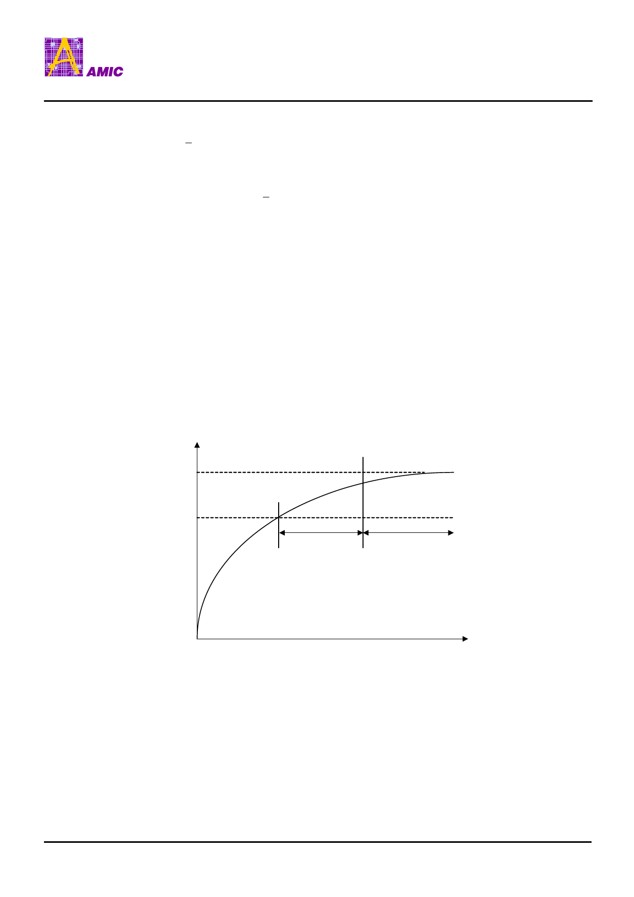
Figure 19. Power-up Timing
VCC
VCC(max)
VCC(min)
tPU
Full Device Access
time
(August, 2007, Version 1.0)
27
AMIC Technology Corp.
Share Link: