ATT3042 查看數據表(PDF) - Unspecified
零件编号
产品描述 (功能)
生产厂家
ATT3042 Datasheet PDF : 80 Pages
| |||
ATT3000 Series Field-Programmable Gate Arrays
Data Sheet
February 1997
Electrical Characteristics (continued)
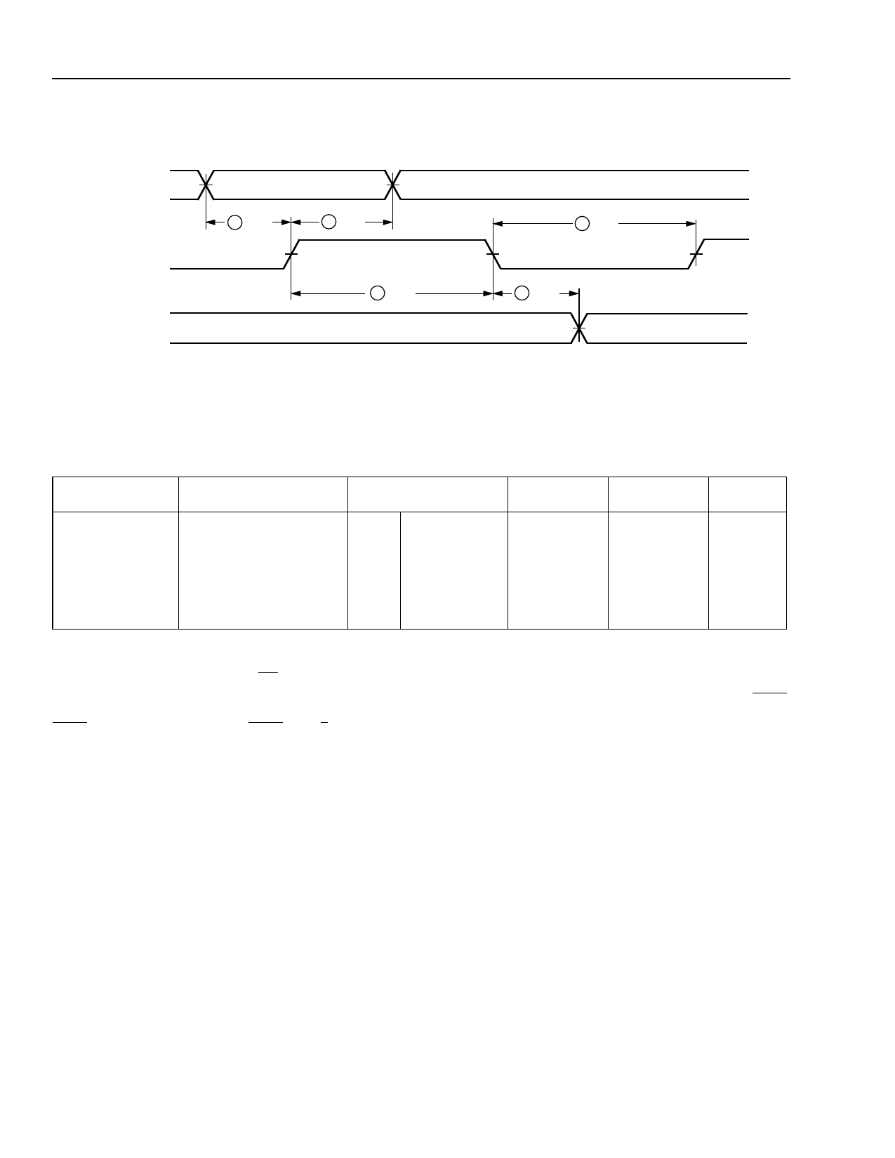
DIN
CCLK
DOUT
(OUTPUT)
BIT N
1 TDCC
2 TCCD
BIT N + 1
5 TCCL
4 TCCH
BIT N – 1
3 TCCO
Figure 39. Slave Mode Switching Characteristics
BIT N
5-3130(F)
Table 29. Slave Mode Switching Characteristics
Commercial: VCC = 5.0 V ± 5%; 0 °C ≤ TA ≤ 70 °C; Industrial: VCC = 5.0 ± 10%, –40 °C ≤ TA ≤ +85 °C.
Signal
Description
Symbol
Min
Max
Unit
CCLK
To DOUT
DIN Setup
DIN Hold
HIGH Time
LOW Time
Frequency
3
TCCO
1
TDCC
2
TCCD
4
TCCH
5
TCCL
—
FCC
—
60
0
0.05
0.05
—
100
ns
—
ns
—
ns
—
µs
5.0
µs
10.0
MHz
Notes:
The maximum limit of CCLK LOW time is caused by dynamic circuitry inside the FPGA device.
Configuration must be delayed until the INIT of all FPGAs is high.
At powerup, VCC must rise from 2.0 V to VCC minimum in less than 25 ms. If this is not possible, configuration can be delayed by holding RESET
low until VCC has reached 4.0 V. A very long VCC rise time of >100 ms, or a nonmonotonically rising VCC, may require a >1 µs high level on
RESET, followed by >6 µs low level on RESET and D/P after VCC has reached 4.0 V.
66
Lucent Technologies Inc.
Share Link: 