UAA3545HL 查看數據表(PDF) - Philips Electronics
零件编号
产品描述 (功能)
生产厂家
UAA3545HL Datasheet PDF : 28 Pages
| |||
Philips Semiconductors
Fully integrated DECT transceiver
Product specification
UAA3545
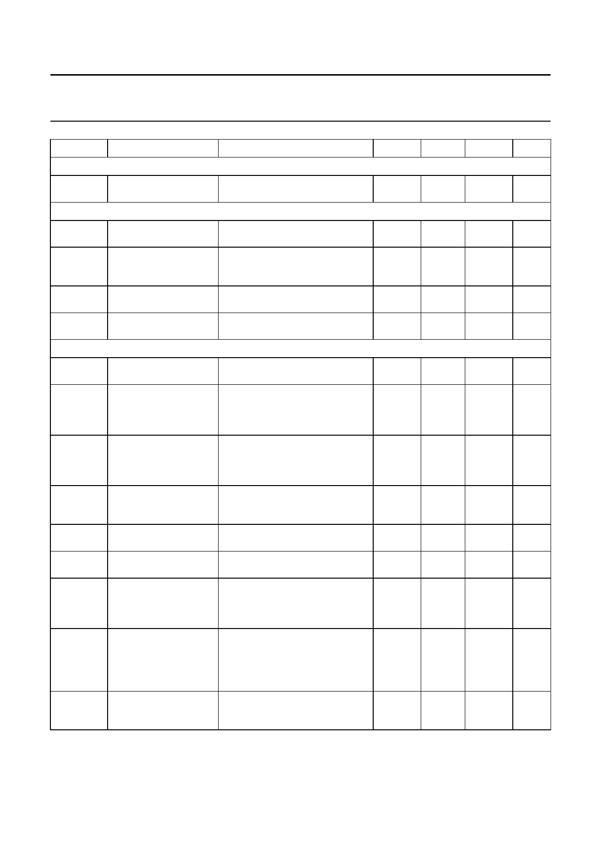
SYMBOL
PARAMETER
CONDITIONS
MIN.
CHARGE-PUMP OUTPUT
Io(CP)
charge-pump output
VCP = 1⁄2VCC
−
current
VCO
fVCO
VCP/VCOtune
oscillator frequency
charge pump input
voltage and VCO tuning
output voltage
defined at transmit output,
Tamb = −10 to +60 °C; note 1
GVCO
VCO tuning input gain defined at transmit output; note 2
(mean value)
GMOD
VCO modulation input defined at transmit output; note 3
gain
1 880
0.3
−
−
Transmit preamplifier
Po(TXA),
Po(TXB)
Ro(TXA),
Ro(TXB)
transmit output power
transmit output
resistance (real part of
the parallel output
impedance)
Tamb = −10 to +60 °C; fVCO = 1880 0
to 1930 MHz; note 1
balanced; expressed at high signal −
level
Co(TXA),
Co(TXB)
transmit output
capacitance (imaginary
part of the parallel
output impedance)
balanced; expressed at high signal −
level
fVCO(feedthru) VCO frequency
referred to Po(TXA), Po(TXB);
−
feedthrough at
fVCO = 1900 MHz; note 1
transmit output
CNR25
carrier-to-noise ratio at carrier offset in closed loop;
−
transmit output
∆f = 25 kHz
CNR4686 carrier-to-noise ratio at carrier offset; ∆f = 4686 kHz
−
transmit output
∆fo(push)
frequency shift due to measured dynamically;
−
supply voltage drop
VCC drop = 100 mV;
VCP/VCOtune = 1.2 V; VMOD = 0;
TX load = 50 Ω; note 1
∆fo(pull)
frequency shift due to frequency pulling measured 20 µs −
disabling the synthesizer after synthesizer disabled;
VCP/VCOtune set by the PLL on
fVCO = 1880.064 MHz; VMOD = 0;
TX load = 50 Ω; note 1
∆fo(drift)
transmit output
notes 1 and 4
−
frequency drift during a
slot
TYP. MAX. UNIT
3.5
−
mA
−
1 930
MHz
−
VCC − 0.3 V
70
−
2.4
−
MHz/V
MHz/V
3
−
200
−
dBm
Ω
0.3
−
pF
−20
−15
dBc
−65
−135
+10
−56
−129
±20
dBc/Hz
dBc/Hz
kHz
+5
±10
kHz
−6
±12
kHz
2001 Sep 06
12
Share Link: 