SIHFP23N50L 查看數據表(PDF) - Vishay Semiconductors
零件编号
产品描述 (功能)
生产厂家
SIHFP23N50L Datasheet PDF : 8 Pages
| |||
IRFP23N50L, SiHFP23N50L
Vishay Siliconix
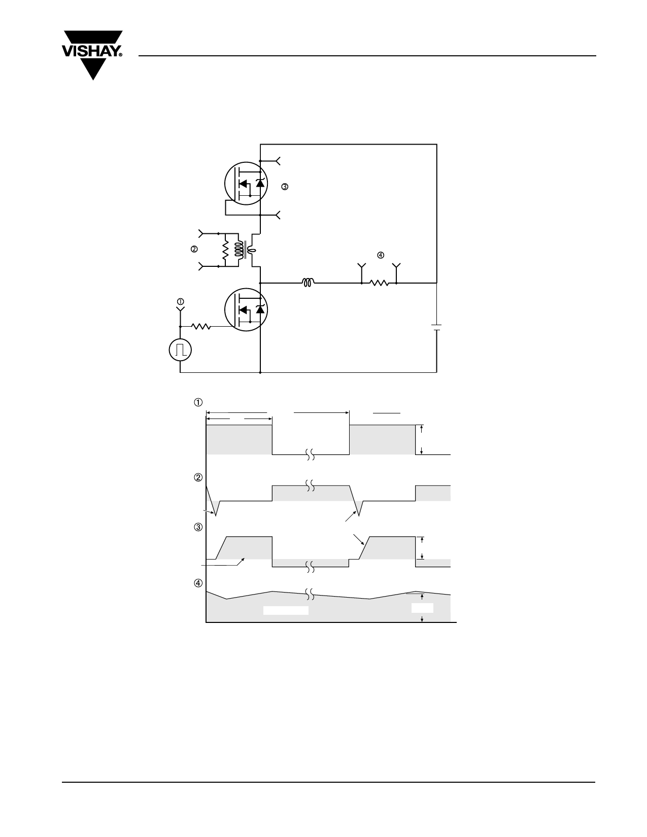
D.U.T
+
-
Peak Diode Recovery dV/dt Test Circuit
+
Circuit Layout Considerations
• Low Stray Inductance
• Ground Plane
• Low Leakage Inductance
Current Transformer
-
-
+
RG
• dV/dt controlled by RG
+
• Driver same type as D.U.T.
• ISD controlled by Duty Factor "D"
- VDD
• D.U.T. - Device Under Test
Driver Gate Drive
P.W.
Period
D=
P.W.
Period
VGS=10V *
D.U.T. ISD Waveform
Reverse
Recovery
Body Diode Forward
Current
Current
dI/dt
D.U.T. VDS Waveform
Diode Recovery
dV/dt
VDD
Re-Applied
Voltage
Body Diode
Inductor Curent
Forward Drop
Ripple ≤ 5%
ISD
* VGS = 5V for Logic Level Devices
Fig. 17 - For N-Channel
Vishay Siliconix maintains worldwide manufacturing capability. Products may be manufactured at one of several qualified locations. Reliability data for Silicon
Technology and Package Reliability represent a composite of all qualified locations. For related documents such as package/tape drawings, part marking, and
reliability data, see http://www.vishay.com/ppg?91209.
Document Number: 91209
S-81352-Rev. A, 16-Jun-08
www.vishay.com
7
Share Link: 