ICM7231 查看數據表(PDF) - Intersil
零件编号
产品描述 (功能)
生产厂家
ICM7231 Datasheet PDF : 16 Pages
| |||
ICM7231, ICM7232
DATA CLOCK Input signal, and when the correct number of
bits has been shifted into the shift register (8 in the
ICM7232), the DATA ACCEPTED Output goes low. Following
this, a low-going pulse at the WRITE input will trigger the
chip to decode the data and store it in the output latches of
the addressed digit/character. After the data is latched at the
outputs, the shift register and the control logic are reset,
returning the DATA ACCEPTED Output high. After this occurs,
a pulse at the WRITE input will not change the outputs, but
will reset the control logic and shift register, assuring that each
data bit will be entered into the correct position in the shift reg-
ister depending on subsequent DATA CLOCK inputs.
The shift register and control logic will also be reset if too
many DATA CLOCK INPUT edges are received; this pre-
vents incorrect data from being decoded. In the ICM7232,
the eleventh clock resets the shift register and control logic.
The recommended procedure for entering data is shown in
the serial input timing diagram, Figure 2. First, when DATA
ACCEPTED is high, send a WRITE pulse. This resets the
shift register and control logic and initializes the chip for the
data input sequence. Next clock in the appropriate number
of correct data and address bits. The DATA ACCEPTED Out-
put may be monitored if desired, to determine when the chip
is ready to output the decoded data. When the correct num-
ber of bits has been entered, and the DATA ACCEPTED Out-
put is low, a pulse at WRITE will cause the data to be
decoded and stored in the latches of the addressed
digit/character. The shift register and control logic are reset,
causing DATA ACCEPTED to return high, and leaving the
chip ready to accept data for the next digit/character.
Note that for the ICM7232 the eleventh clock resets the shift
register and control logic, but the DATA ACCEPTED Output
goes low after the eighth clock. This allows the user to
abbreviate the data to eight bits, which will write the correct
character to the 7-segment display, but will leave the annun-
ciators off, as shown in Figure 3.
If only AN2 is to be turned on, nine bits are clocked in; if AN1
is to be turned on, all ten bits are used.
The DATA ACCEPTED Output will drive one low-power
Schottky TTL input, and has equal current drive capability
pulling high or low.
Note that in the serial Input devices, it is possible to address
digits/characters which don’t exist. As shown in Table 2
when an incorrect address is applied together with a WRITE
pulse, none of the outputs will be changed.
Display Fonts and Output Codes
The standard versions of the ICM7231 and ICM7232 chips are
programmed to drive a 7-segment display plus two annuncia-
tors per digit. See Table 3 for annunciator input controls.
The “A” and “B” suffix chips place both annunciators on BP3.
The display connections for one digit of this display are
shown in Figure 13. The “A” devices decode the input data
into a hexadecimal 7-segment output, while the “B” devices
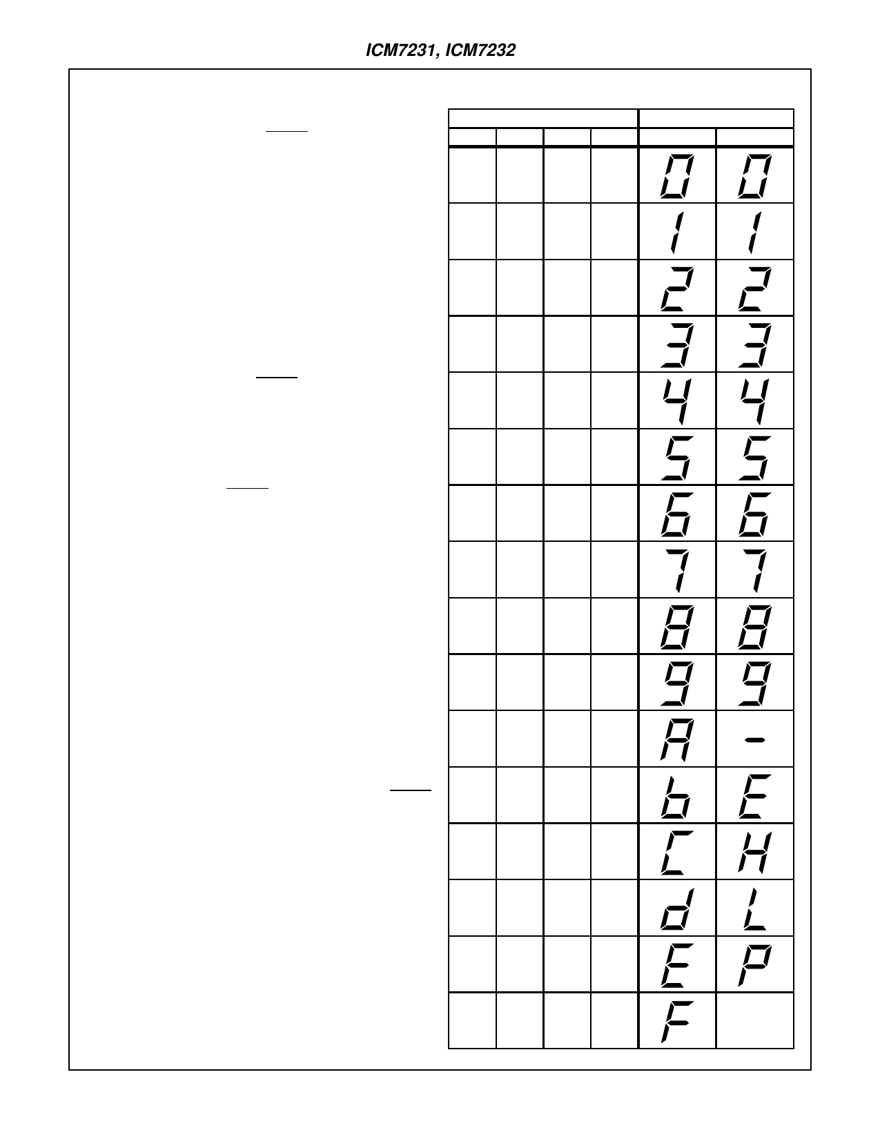
supply Code B outputs (see Table 1).
The “C” devices place the left hand annunciator on BP1 and
the right hand annunciator (usually a decimal point) on BP3.
(See Figure 14). The “C” devices provide only a “Code B”
output for the 7 segments.
TABLE 1. BlNARY DATA DECODING ICM7231 AND ICM7232
BD3
0
CODE INPUT
BD2 BD1
0
0
BD0
0
DISPLAY OUTPUT
HEX
CODE B
0
0
0
1
0
0
1
0
0
0
1
1
0
1
0
0
0
1
0
1
0
1
1
0
0
1
1
1
1
0
0
0
1
0
0
1
1
0
1
0
1
0
1
1
1
1
0
0
1
1
0
1
1
1
1
0
1
1
1
1
BLANK
9-30
Share Link: 