TDA16831 查看數據表(PDF) - Infineon Technologies
零件编号
产品描述 (功能)
生产厂家
TDA16831 Datasheet PDF : 21 Pages
| |||
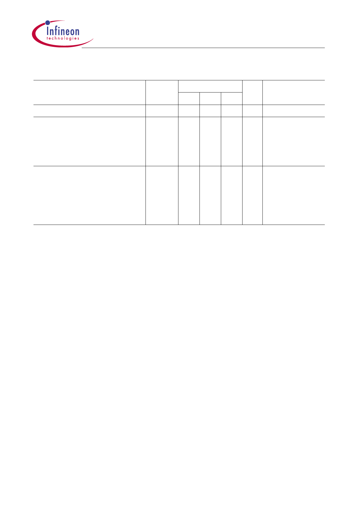
TDA16831-4
PWM Section
Parameter
Symbol Limit Values Unit Test Conditions
min. typ. max.
Duty Cycle
D
Trans Impedance ∆VFB / ∆IDrain 2)
OP Gain Bandwidth 1)
OP Phase Margin 1)
ZPWM
ZPWM
ZPWM
Bw
Phim
VFB Operating Range min. Level VFBmin
VFB Operating Range max. Level VFBmax
Feedback Resistance
RFB
Temperature Coefficient RFB
RFBTK
Internal Reference Voltage
Vrefint
Temperature Coefficient Vrefint Vreftk
0
4
2
1.3
2
70
0.45
3.5
3.0 3.7
600
5.3 5.5
0.2
0.5
V/A TDA16831/G
V/A TDA16832/G
V/A TDA16833/G/4
MHz
degree
0.85
4.8
4.9
V
V
KΩ
ppm/°C
for D = 0
Ics = 0.95 Icsth
5.7 V
mV/°C
1) Guaranteed by design
2) For discontinuous mode the VFB is described by:
VFB
=
ZPWM
×
I---P---K-
ton
×
æ
ç
ç
to
n
è
–
T1
+
T1
×
e ---T-t-o--1--n- ÷÷ö
+
0.6
×
æ
çç 1
è
–
e---Tt--o--2--n-÷÷ö
T1 = 850 ns; T2 = 200 ns
Data Sheet
12
1999-12-10
Share Link: 