LB11923V-MPB-E 查看數據表(PDF) - ON Semiconductor
零件编号
产品描述 (功能)
生产厂家
LB11923V-MPB-E Datasheet PDF : 23 Pages
| |||
LB11923V
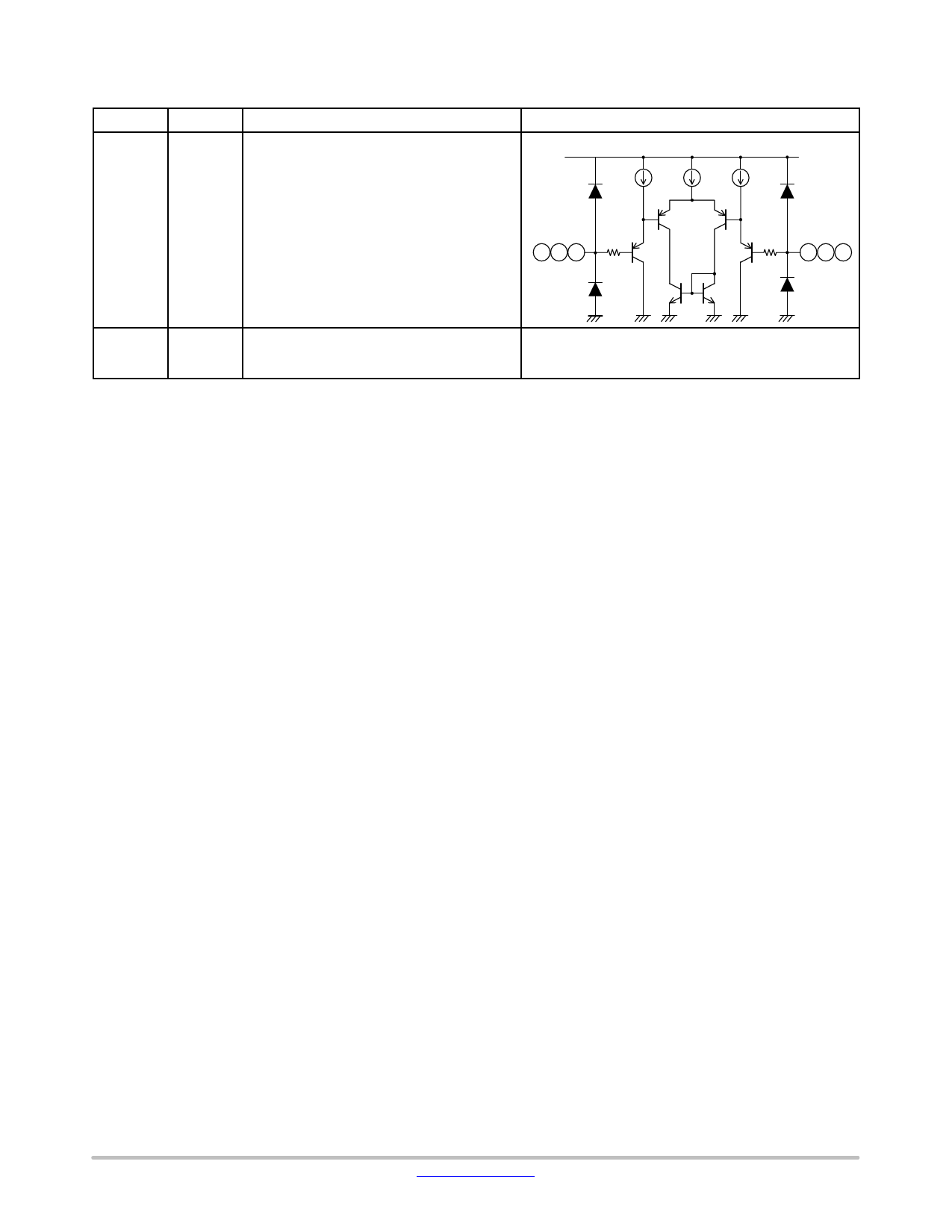
PIN FUNCTIONS (continued)
Pin No.
Pin
Functions
39
IN3−
Hall−effect device inputs.
40
IN3+
The input is seen as a high-level input when
41
IN2−
IN+ > IN–, and as a low-level input for the oppo-
42
IN2+
site state.
43
IN1−
If noise on the Hall-effect device signals is
44
IN1+
a problem, insert capacitors between the
corresponding IN+ and IN– inputs.
The logic high state indicates that VIN+ > VIN–
VCC1
Equivalent Circuit
500 W
40 42 44
500 W
39 41 43
12
NC
These are unconnected pins, and can be used
18
for wiring.
26
www.onsemi.com
14
Share Link: 