TDA2541 查看數據表(PDF) - STMicroelectronics
零件编号
产品描述 (功能)
生产厂家
TDA2541 Datasheet PDF : 7 Pages
| |||
TDA2540 - TDA2541
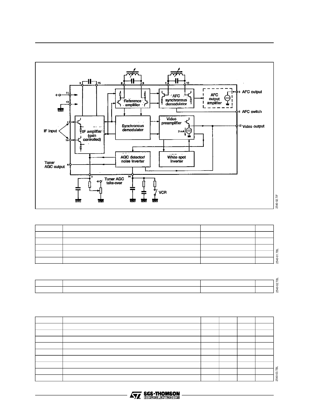
BLOCK DIAGRAM
ABSOLUTE MAXIMUM RATINGS
Symbol
V (11–13)
V (4–13)
Ptot
Tstg
Ta mb
Parameter
Supply Voltage
Tuner A.G.C. Voltage
Power Dissipation
Storage Temperature
Operating Ambient Temperature
THERMAL DATA
Symbol
Rth (j-a)
Parameter
Junction - ambient Thermal Resistance
ELECTRICAL OPERATING CHARACTERISTICS
Tamb = 25oC ; V11–13 = 12V; f = 38.9MHz (unless otherwise specified)
Symbol
V11-13
I11
V1-16
V12-13
Z1-16
V12-13
V12-13
∆GV
Parameter
Supply Voltage Range
Supply Current
IF Input Voltage Sensitivity
Max Input Voltage (Pins 1-16)
Video Output Voltage
Differential Input Impedance (in parallel with 2pF)
Zero Signal Output Level
Top Synchro Output Level
IF Voltage Gain Control Range
2/7
Value
Unit
13.8
V
12
V
900
mW
– 55 to + 125
°C
0 to + 70
°C
Value
70
Unit
°C/W
Min.
10.2
60
5.7
2.9
52
Typ.
12
50
85
140
2.7
2
6
3.07
64
Max.
13.8
60
180
6.3
3.2
Unit
V
mA
µVRMS
mV
Vpp
kΩ
V
V
dB
Share Link: 