10XSD200 查看數據表(PDF) - Freescale Semiconductor
零件编号
产品描述 (功能)
生产厂家
10XSD200 Datasheet PDF : 60 Pages
| |||
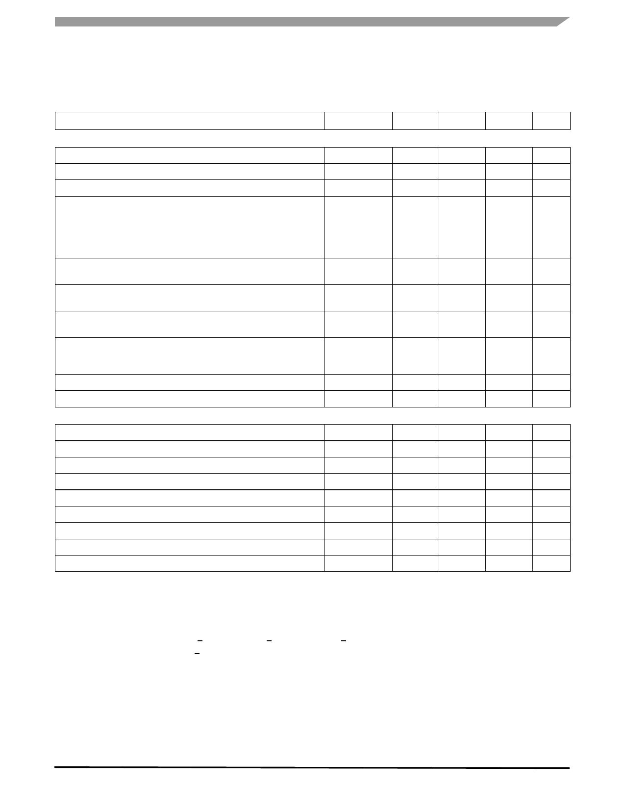
ELECTRICAL CHARACTERISTICS
STATIC ELECTRICAL CHARACTERISTICS
Table 3. Static Electrical Characteristics (continued)
Unless specified otherwise: 8.0 V VPWR 36 V, 3.0 V VDD 5.5 V, - 40 C TA 125 C, GND = 0 V. Typical values are
average values evaluated under nominal conditions TA = 25 °C, VPWR = 28 V & VDD = 5.0 V, unless specified otherwise.
parameter
Symbol
Min
Typ
Max
Unit
ELECTRICAL CHARACTERISTICS OF THE OUTPUT STAGE (HS0 AND HS1) (CONTINUED)
Current Sense Clamping Voltage (condition: R(CSNS) > 10 kOhm)
VCL(CSNS)
5.5
–
7.5
V
OpenLoad detection Current threshold in OFF state (21)
IOLD(OFF)
30
–
100
A
OpenLoad Fault Detection Voltage Threshold (21)
VOLD(THRES)
4.0
–
5.5
V
OpenLoad detection Current threshold in ON state (see OpenLoad
Detection In On State (OL_ON)):
IOLD(ON)
CSNS_ratio bit = 0
CSNS_ratio bit = 1 (fast slew rate SR[1:0] = 10 mandatory for this
function)
80
300
600
mA
5.0
7.0
10
Time period of the periodically activated OpenLoad in ON state detection
for CSNS_ratio bit = 1
tOLLED
105
150
195
ms
Output Shorted-to-VPWR Detection Voltage Threshold (channel in OFF
VOSD(THRES)
VPWR-1.2 VPWR-0.8 VPWR-0.4
V
state)
Switch turn-on threshold for Negative Output Voltages (protects against
negative transients) - (measured at IOUT = 100 mA, Channel in OFF state)
Switch turn-on threshold for Negative Output Voltages difference from
one channel to the other in parallel mode - (measured at IOUT = 100 mA,
Channel in OFF state)
VCL
VCL
-35
–
-24
V
-2.0
–
+2.0
V
Switching State (On/Off) discrimination thresholds
VHS_TH
0.45*VPWR 0.5*VPWR 0.55*VPWR
V
Shutdown temperature (Power MOSFET junction; 6.0 V < VPWR < 58 V)
TSD
160
175
190
C
ELECTRICAL CHARACTERISTICS OF THE CONTROL INTERFACE PINS
Logic Input Voltage, High(22)
VIH
2.0
–
5.5
V
Logic Input Voltage, Low(22)
VIL
-0.3
–
0.8
V
Wake-up Threshold Voltage (IN[0:1] and RSTB)(23)
VWAKE
1.0
–
2.2
V
Internal Pull-down Current Source (on inputs: CLOCK, SCLK and SI)(24)
IDWN
5.0
–
20
A
Internal Pull-up Current Source (input CSB)(25)
IUP_CSB
5.0
–
20
A
Internal Pull-up Current Source (input CONF[0:1])(26)
IUP_CONF
25
–
100
A
Capacitance of SO, FSB and FSOB pins in Tri-state
CSO
–
–
20
pF
Internal Pull-down Resistance (RSTB and IN[0:1])
Input Capacitance(27)
RDWN
CIN
125
250
500
k
–
4.0
12
pF
Notes:
21. Minimum required value of OpenLoad impedance for detection of OpenLoad in OFF-state: 200 k.(VOLD(THRES) = VHS @ IOLD(OFF))
22. High and low voltage ranges apply to SI, CSB, SCLK, RSTB, IN[0:1] and CLOCK input signals. The IN[0:1] signals may be derived from
VPWR and can tolerate voltages up to 58 V.
23. Voltage above which the device wakes up
24. Pull-down current-value for VSI > 0.8 V and VSCLK > 0.8 V and VCLOCK > 0.8 V.
25. Pull-up current-value for VCSB < 2.0 V. CSB has an internal pull-up current source connected to VDD.
26. Pins CONF[0:1] are connected to an internal current source, connected itself to an internal voltage regulator (VREG ~ 3.0 V).
27. Input capacitance of SI, CSB, SCLK, RSTB, IN[0:1], CONF[0:1], and CLOCK pins. This parameter is guaranteed by the manufacturing
process but is not tested in production.
Analog Integrated Circuit Device Data
Freescale Semiconductor
10XSD200
13
Share Link: 