TTSI1K16T 查看數據表(PDF) - Agere -> LSI Corporation
零件编号
产品描述 (功能)
生产厂家
TTSI1K16T Datasheet PDF : 64 Pages
| |||
TTSI1K16T
1024-Channel, 16-Highway Time-Slot Interchanger
Preliminary Data Sheet
February 1999
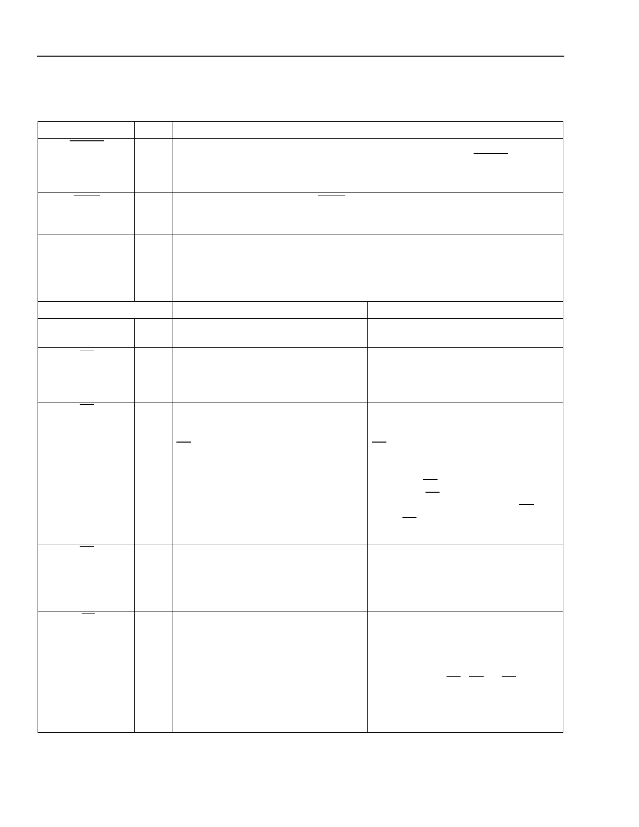
Pin Information (continued)
Table 4. TTSI1K16T Pin Descriptions
Symbol
Type*
Description
RESET
TEST
I Reset (Active-Low). A low on this pin resets the TTSI1K16T. It is asynchronous to
any other clock or input signal. All flip-flops will be cleared when RESET is low. All
counters, state machines, and configuration registers will be set to the default state
following a reset.
Iu Test (Active-Low). When low, TEST causes the output and bidirectional pins of the
TTSI1K16T device to be in a high-impedance state. This pin has an internal pull-up
resistor.
MM
I Microprocessor Mode. When MM = 0, the TTSI1K16T uses an asynchronous type
handshake (equal to mode 1 of the Lucent dual T1/E1 terminator devices). When
MM = 1, the TTSI1K16T uses a synchronous type handshake which requires a host
processor clock (PCLK) input. Both modes use a demultiplexed address and data
bus.
—
Synchronous Mode (MM = 1)
Asynchronous Mode (MM = 0)
PCLK
I Host Processor Clock. Valid from
0 MHz to 65 MHz.
Unused. Must be either tied high or low.
AS
I Address Valid (Active-Low). Valid for Address Valid (Active-Low). Indicates
one PCLK cycle. Indicates the start of a a valid address for a processor access.
processor access.
Must be held low for the duration of the
access.
CS
I Chip Select (Active-Low). This pin is Chip Select (Active-Low). This pin is
asserted low to enable any transfers
asserted low to enable any transfers
through the microprocessor interface. through the microprocessor interface.
CS should be a decode of all address CS should be a decode of all address
and cycle type signals defining the mem- and cycle type signals defining the mem-
ory map location of the TTSI1K16T.
ory map location of the TTSI1K16T. In
this mode, CS is used to control the
tristating of DT at the end of the cycle.
The input timing requirement of CS rela-
tive to AS is described in the Timing
Characteristics section on page 54.
DS
I Not Used. Must be tied high.
Data Valid (Active-Low). Indicates valid
data during processor writes. The
TTSI1K16T will start driving D[7—0]
when this signal is asserted during pro-
cessor reads.
DT
O Data Transfer Acknowledge (Active- Data Transfer Acknowledge (Active-
Low). Active for one PCLK cycle. Indi- Low). Indicates that data has been writ-
cates that data has been written during ten during processor writes. Indicates
processor writes. Indicates that read
that read data is valid during processor
data is valid during processor reads.
reads. Once driven active, this signal is
An external pull-up is required on this
output.
held active until AS , DS, or CS is
removed.
An external pull-up is required on this
output.
* Iu indicates internal 100 kΩ pull-up resistor, and Id indicates 17.5 kΩ pull-down resistor.
10
Lucent Technologies Inc.
Share Link: 