AU5783(2001) 查看數據表(PDF) - Philips Electronics
零件编号
产品描述 (功能)
生产厂家
AU5783 Datasheet PDF : 14 Pages
| |||
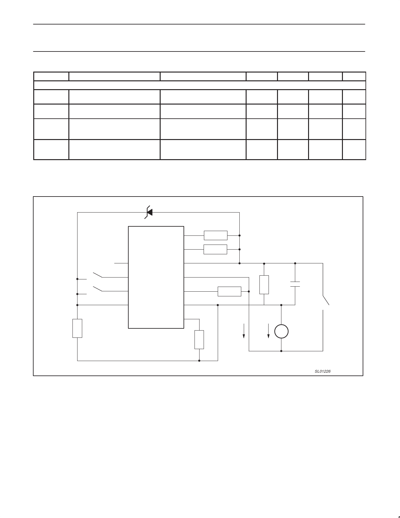
Philips Semiconductors
J1850/VPW transceiver with supply control function
Preliminary specification
AU5783
DYNAMIC CHARACTERISTICS
7 V < VBAT < 16 V; –40°C < Tamb < +125°C; –2 V < Vbus < +9 V; 1.4 kΩ < Rld < 12 kΩ
BUS: 250 Ω < RL < 1.6 kΩ; 3 nF < CL < 17 nF; 1.7 µs < (RL * CL) < 5.2 µs
Bus load A: RL = 1.38 kΩ, CL = 3.3 nF; Bus load B: RL = 300 Ω, CL = 16.5 nF
R/F pin: Rs = 56 kΩ ± 1%; INH loaded with 100 kΩ and 30 pF to GND
RX pin: Rd = 3.9 kΩ to 5 V; CL = 30 pF to GND; NSTB = 5 V; 4X/LOOP = 0 V
Typical values reflect the approximate average value at VBAT = 13 V and Tamb = 25°C, unless otherwise specified.
NSTB and 4X/LOOP rise and fall times < 10 ns.
SYMBOL
PARAMETER
CONDITIONS
MIN.
CTX
TX input capacitance
Note 1
INH output function
tinhoff
INH turn-off delay
BUS = 0 V, LWAKE = VBAT or 0 V, go to sleep command,
measured from NSTB = 0.9 V to INH = 3.5 V
tinhonl
LWAKE to INH turn-on delay
NSTB = 0 V, BUS = 0 V, measured from LWAKE = 3 V to
INH = 3.5 V
tinhonr BUS to INH turn-on delay
sleep mode, LWAKE = VBAT, measured from BUS = 3.875 V to
INH = 3.5 V
BUS output function
tBOon;
tBOoff
tBrA
tBrB
tBfA
tBfB
tir
Delay TX to BUS rising and
falling edge
BUS voltage rise time
BUS voltage rise time
BUS output voltage fall time
BUS output voltage fall time
BUS output current rise time
from TX = 2.5 V to BUS = 3.875 V; bus load A and bus load B 13
bus load A, 9 V < VBAT < 16 V, measured at 1.5 V and 6.25 V 11
bus load B, 9 V < VBAT < 16 V, measured at 1.5 V and 6.25 V 11
bus load A, 9 V < VBAT < 16 V, measured at 1.5 V and 6.25 V 11
bus load B, 9 V < VBAT < 16 V, measured at 1.5 V and 6.25 V 11
bus load B connected to –2 V,
4
9 V < VBAT < 16 V, measured at 20% and 80% of load
capacitor current
tif
BUS output current fall time
bus load B connected to –2 V,
4
9 V < VBAT < 16 V, measured at 20% and 80% of load
capacitor current
twBh
BUS high pulse width
TX = high for 64 µs, bus load condition A, 9 V < VBAT < 16 V; 35
minimum width measured at BUS = 6.25 V, maximum width
measured at BUS = 1.5 V
BHRM
BUS output voltage harmonic
content; normal mode
f = 530 kHz to 1670 kHz, bus load B connected to –2 V,
TX = 7.81 kHz, 50% duty cycle, 9 V < VBAT < 16 V, Note 1
tBO4Xon; TX to BUS delay in 4X mode 4X/LOOP = 1 V, bus load B,
0.5
tBO4Xoff
9 V < VBAT < 16 V, from TX = 1.8 V to BUS = 3.875 V
tpon;
Delay TX to RX rising and
measured from 1.8 V on TX to 2.5 V on RX
13
tpoff
falling edge in normal mode
tplbon; Delay TX to RX rising and
NSTB = 5 V, 4X = floating, measured from 1.8 V on TX to
13
tplboff
falling edge in loop-back mode 2.5 V on RX
BUS input function
tDRXon; BUS input delay time, rising
measured from VBUS = 3.875 V to VRX = 2.5 V
0.2
tDRXoff and falling edge
ttRX
RX output transition time, rising NSTB = 5 V, measured at 10% and 90% of waveform
and falling edge
ttRXsl
RX output transition time in
NSTB = 0 V, measured at 10% and 90% of waveform
standby and sleep mode, rising
and falling edge
tDRXsl
BUS to RX delay in sleep and NSTB = 0 V, LWAKE = VBAT, measured from BUS = 3.875 V 8
standby modes
to RX = 2.5 V
NOTES:
1. This parameter is characterized but not subject to production test.
TYP. MAX. UNIT
15
pF
200 µs
100 µs
60
µs
22
µs
18
µs
18
µs
18
µs
18
µs
µs
µs
93
µs
70
dBµV
5
µs
25
µs
25
µs
2
µs
1
µs
5
µs
60
µs
2001 Feb 15
10
Share Link: 