LC75829PW 查看數據表(PDF) - SANYO -> Panasonic
零件编号
产品描述 (功能)
生产厂家
LC75829PW Datasheet PDF : 22 Pages
| |||
LC75829PE, 75829PW
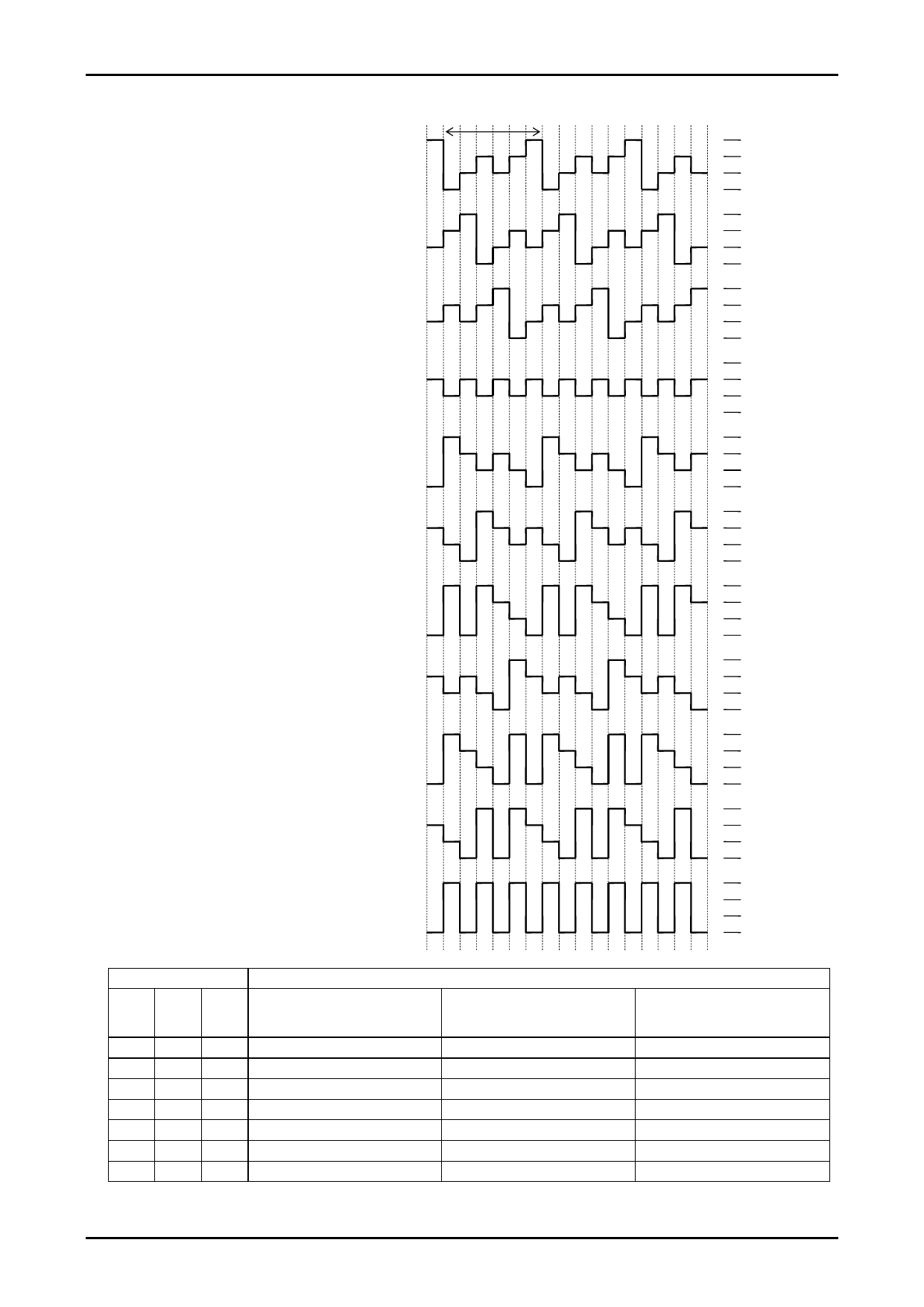
Output waveforms (1/3-Duty 1/3-Bias Drive Scheme)
fo[Hz]
COM1
COM2
COM3
LCD driver output when all LCD segments
corresponding to COM1, COM2, and COM3
are off.
LCD driver output when only LCD segments
corresponding to COM1 are on.
LCD driver output when only LCD segments
corresponding to COM2 are on.
LCD driver output when LCD segments
corresponding to COM1 and COM2 are on.
LCD driver output when only LCD segments
corresponding to COM3 are on.
LCD driver output when LCD segments
corresponding to COM1 and COM3 are on.
LCD driver output when LCD segments
corresponding to COM2 and COM3 are on.
LCD driver output when all LCD segments
corresponding to COM1, COM2, and COM3
are on.
VDD
VDD1
VDD2
0V
VDD
VDD1
VDD2
0V
VDD
VDD1
VDD2
0V
VDD
VDD1
VDD2
0V
VDD
VDD1
VDD2
0V
VDD
VDD1
VDD2
0V
VDD
VDD1
VDD2
0V
VDD
VDD1
VDD2
0V
VDD
VDD1
VDD2
0V
VDD
VDD1
VDD2
0V
VDD
VDD1
VDD2
0V
Control data
Frame frequency fo[Hz]
FC0 FC1 FC2
Internal oscillator operating mode
(The control data OC is 0,
fosc=300[kHz]typ)
External clock operating mode
(The control data OC is 1
and EXF is 0, fCK1=300[kHz]typ)
External clock operating mode
(The control data OC is 1
and EXF is 1, fCK2=38[kHz]typ)
0
0
0
fosc/6144
fCK1/6144
fCK2/768
0
0
1
fosc/4608
fCK1/4608
fCK2/576
0
1
0
fosc/3072
fCK1/3072
fCK2/384
0
1
1
fosc/2304
fCK1/2304
fCK2/288
1
0
0
fosc/1536
fCK1/1536
fCK2/192
1
0
1
fosc/1152
fCK1/1152
fCK2/144
1
1
0
fosc/768
fCK1/768
fCK2/96
Note: When is setting (FC0,FC1,FC2)=(1,1,1), the frame frequency is same as frame frequency at the time of the
(FC0,FC1,FC2)=(0,1,0) setting (fosc/3072, fCK1/3072, fCK2/384).
No.A1462-18/22
Share Link: 