NTD20N06 查看數據表(PDF) - ON Semiconductor
零件编号
产品描述 (功能)
生产厂家
NTD20N06 Datasheet PDF : 8 Pages
| |||
NTD20N06
Power MOSFET
20 Amps, 60 Volts, N−Channel DPAK
Designed for low voltage, high speed switching applications in
power supplies, converters and power motor controls and bridge
circuits.
Features
• Pb−Free Packages are Available
• Lower RDS(on)
• Lower VDS(on)
• Lower Capacitances
• Lower Total Gate Charge
• Lower and Tighter VSD
• Lower Diode Reverse Recovery Time
• Lower Reverse Recovery Stored Charge
Typical Applications
• Power Supplies
• Converters
• Power Motor Controls
• Bridge Circuits
MAXIMUM RATINGS (TJ = 25°C unless otherwise noted)
Rating
Symbol Value Unit
Drain−to−Source Voltage
Drain−to−Gate Voltage (RGS = 10 MW)
Gate−to−Source Voltage
− Continuous
− Non−repetitive (tpv10 ms)
Drain Current
− Continuous @ TA = 25°C
− Continuous @ TA = 100°C
− Single Pulse (tpv10 ms)
Total Power Dissipation @ TA = 25°C
Derate above 25°C
Total Power Dissipation @ TA = 25°C (Note 1)
Total Power Dissipation @ TA = 25°C (Note 2)
Operating and Storage Temperature Range
VDSS
VDGR
VGS
VGS
ID
ID
IDM
PD
TJ, Tstg
60
60
"20
"30
20
10
60
60
0.40
1.88
1.36
−55 to
175
Vdc
Vdc
Vdc
Adc
Apk
W
W/°C
W
W
°C
Single Pulse Drain−to−Source Avalanche
Energy − Starting TJ = 25°C
(VDD = 25 Vdc, VGS = 10 Vdc,
L = 1.0 mH, IL(pk) = 18.4 A, VDS = 60 Vdc)
Thermal Resistance
− Junction−to−Case
− Junction−to−Ambient (Note 1)
− Junction−to−Ambient (Note 2)
Maximum Lead Temperature for Soldering
Purposes, 1/8″ from case for 10 seconds
EAS
RqJC
RqJA
RqJA
TL
170 mJ
°C/W
2.5
80
110
260 °C
Maximum ratings are those values beyond which device damage can occur.
Maximum ratings applied to the device are individual stress limit values (not
normal operating conditions) and are not valid simultaneously. If these limits
are exceeded, device functional operation is not implied, damage may occur
and reliability may be affected.
1. When surface mounted to an FR4 board using the minimum recommended
pad size.
2. When surface mounted to an FR4 board using the 0.5 sq in drain pad size.
© Semiconductor Components Industries, LLC, 2004
1
August, 2004 − Rev. 6
http://onsemi.com
V(BR)DSS
60 V
RDS(on) TYP
37.5 mW
ID MAX
20 A
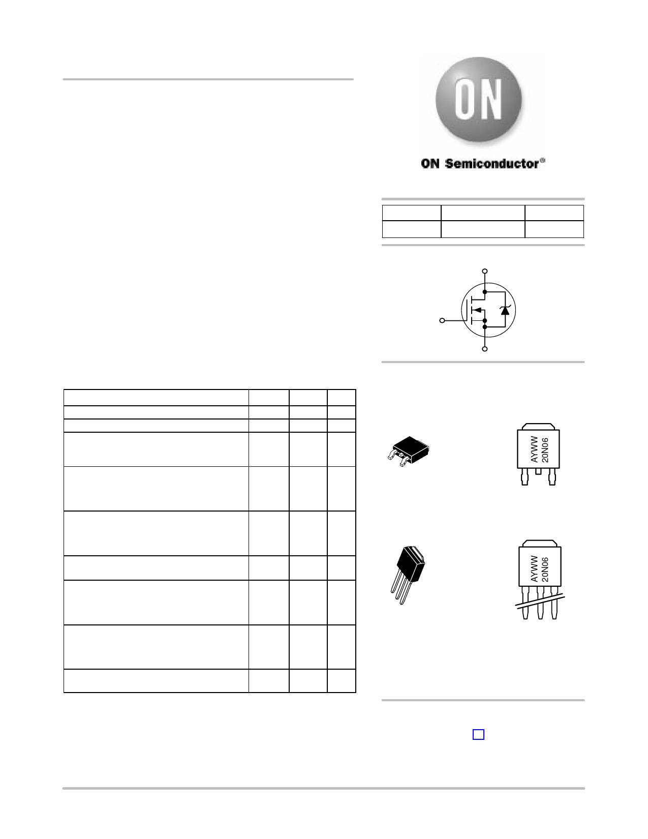
N−Channel
D
G
S
4
12
3
MARKING
DIAGRAMS
4
Drain
DPAK
CASE 369C
STYLE 2
1
Gate
2
Drain
3
Source
4
1
2
3
DPAK−3
CASE 369D
STYLE 2
4
Drain
12 3
Gate Drain Source
20N06
A
Y
WW
= Device Code
= Assembly Location
= Year
= Work Week
ORDERING INFORMATION
See detailed ordering and shipping information in the package
dimensions section on page 2 of this data sheet.
Publication Order Number:
NTD20N06/D
Share Link: 