HD404394 查看數據表(PDF) - Hitachi -> Renesas Electronics
零件编号
产品描述 (功能)
生产厂家
HD404394 Datasheet PDF : 100 Pages
| |||
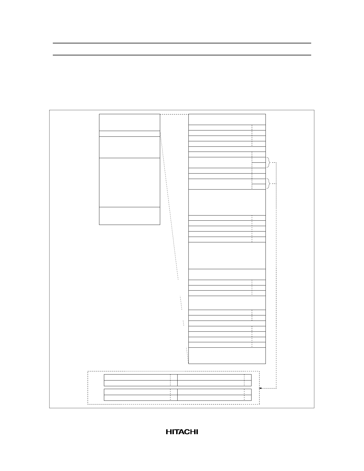
HD404344R Series/HD404394 Series
RAM Memory Map
The MCU RAM contains 256 digits × 4 bits which is used for the memory registers, and the data and stack
areas. The interrupt control bits area, special register area, and the register flag area are mapped into the
RAM memory. The RAM memory area is shown in figure 2 and explained as follows.
$000
$040
$050
$100
RAM-mapped registers
Memory registers (MR)
Data (176 digits)
Not used
$3C0
$3FF
Stack (64 digits)
$000
$003
Interrupt control bits area
$004 Port mode register A (PMRA) W
$005 Serial mode register
(SMR) W
$006 Serial data register lower (SRL) R/W
$007 Serial data register upper (SRU) R/W
$008
Not used
$009 Timer mode register B1 (TMB1) W
$00A Timer B
(TRBL/TWBL) R/W *
$00B
(TRBU/TWBU) R/W
$00C Miscellaneous register (MIS) W
$00D Timer mode register C (TMC) W
$00E Timer C
$00F
(TRCL/TWCL) R/W
(TRCU/TWCU) R/W
Not used
$016 A/D channel register
(ACR) W
$017 A/D data register lower (ADRL) R
$018 A/D data register upper (ADRU) R
$019 A/D mode register 1 (AMR1) W
$01A A/D mode register 2 (AMR2) W
Not used
Note: * Two registers are mapped
on the same area ($00A,
$00B, $00E, $00F).
R: Read only
W: Write only
R/W: Read/write
$020
$023
Register flag area
$024 Port mode register B (PMRB) W
$025 Port mode register C (PMRC) W
$026 Timer mode register B2 (TMB2) W
Not used
$02C Port D0–D3 DCR
(DCD0) W
$02D Port D4, D5 DCR
(DCD1) W
Not used
$030 Port R0 DCR
(DCR0) W
$031 Port R1 DCR
(DCR1) W
$032 Port R2 DCR
(DCR2) W
$033 Port R3 DCR
(DCR3) W
$03F
Not used
$00A Timer read register B lower (TRBL) R Timer write register B lower (TWBL) W
$00B Timer read register B upper (TRBU) R Timer write register B upper (TWBU) W
$00E Timer read register C lower (TRCL) R Timer write register C lower (TWCL) W
$00F Timer read register C upper (TRCU) R Timer write register C upper (TWCU) W
Figure 2 RAM Memory Map
16
Share Link: 