DS1744WP120 查看數據表(PDF) - Unspecified
零件编号
产品描述 (功能)
生产厂家
DS1744WP120 Datasheet PDF : 19 Pages
| |||
DS1744/DS1744P
Y2K-Compliant, Nonvolatile Timekeeping RAMs
PACKAGES
The DS1744 is available in two packages (28-pin encapsulated DIP and 34-pin PowerCap module). The 28-pin EDIP module
integrates the crystal, lithium energy source, and silicon all in one package. The 34-pin PowerCap module board is designed with
contacts for connection to a separate PowerCap (DS9034PCX) that contains the crystal and battery. This design allows the
PowerCap to be mounted on top of the DS1744P after the completion of the surface-mount process. Mounting the PowerCap
after the surface-mount process prevents damage to the crystal and battery due to the high temperatures required for solder
reflow. The PowerCap is keyed to prevent reverse insertion. The PowerCap module board and PowerCap are ordered separately
and shipped in separate containers. The part number for the PowerCap is DS9034PCX.
CLOCK OPERATIONS—READING THE CLOCK
While the double-buffered register structure reduces the chance of reading incorrect data, internal updates to the DS1744 clock
registers should be halted before clock data is read to prevent reading of data in transition. However, halting the internal clock
register updating process does not affect clock accuracy. Updating is halted when a 1 is written into the read bit, bit 6 of the
century register (Table 2). As long as a 1 remains in that position, updating is halted. After a halt is issued, the registers reflect the
count, that is, day, date, and time that was current at the moment the halt command was issued. However, the internal clock
registers of the double-buffered system continue to update so that the clock accuracy is not affected by the access of data. All the
DS1744 registers are updated simultaneously after the internal clock-register updating process has been re-enabled. Updating is
within a second after the read bit is written to 0. The READ bit must be a 0 for a minimal of 500µs to ensure the external registers
are updated.
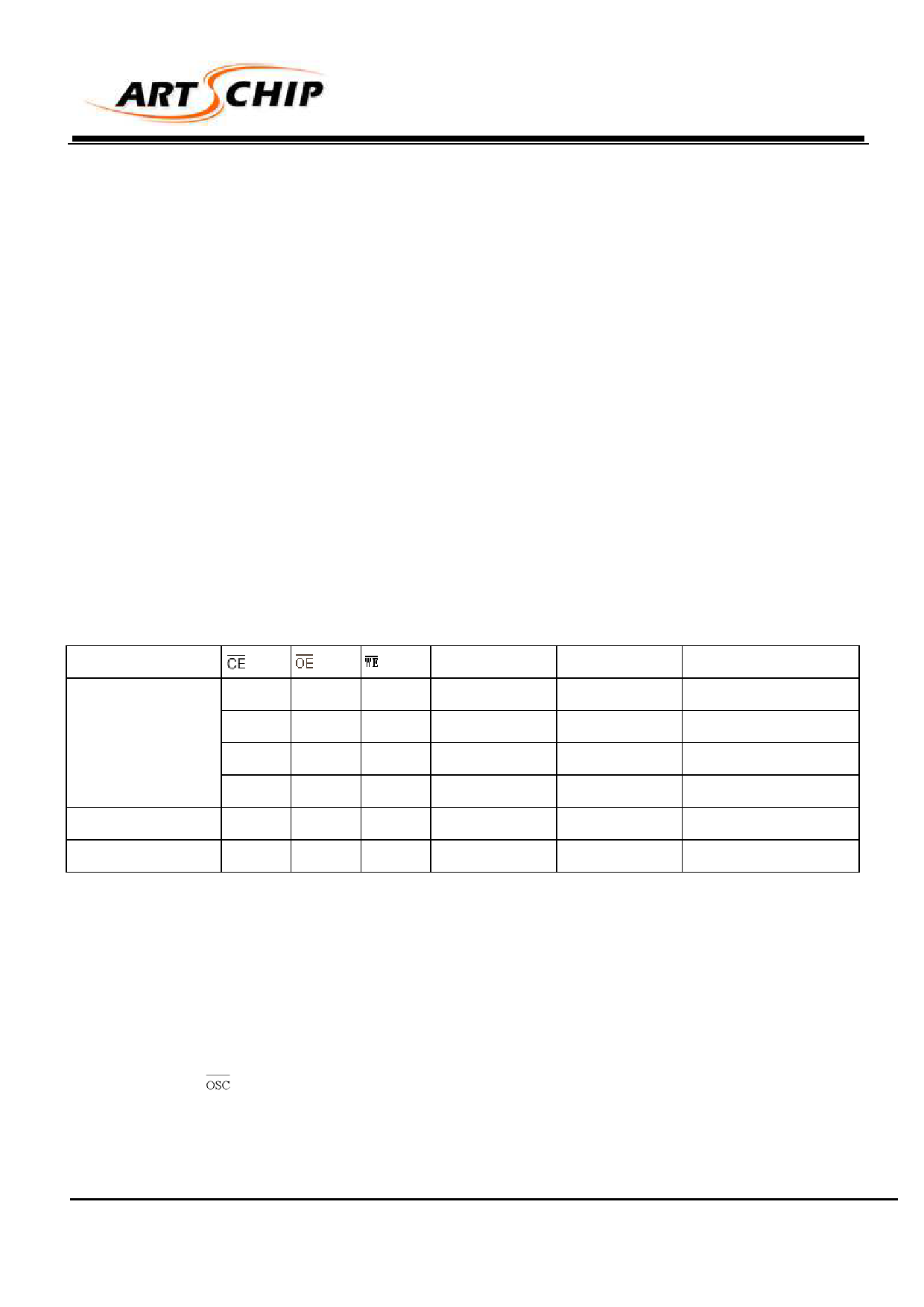
Table 1. Truth Table
VCC
VCC > VPF
VSO < VCC < VPF
VCC < VSO < VPF
MODE
VIH
X
X
Deselect
VIL
X
VIL
Write
VIL
VIL
VIH
Read
VIL
VIH
VIH
Read
X
X
X
Deselect
X
X
X
Deselect
DQ
High-Z
Data In
Data Out
High-Z
High-Z
High-Z
POWER
Standby
Active
Active
Active
CMOS Standby
Data-Retention Mode
SETTING THE CLOCK
As shown in Table 2, bit 7 of the century register is the write bit. Setting the write bit to a 1, like the read bit, halts updates to the
DS1744 registers. The user can then load them with the correct day, date, and time data in 24-hour BCD format. Resetting the
write bit to a 0 then transfers those values to the actual clock counters and allows normal operation to resume.
STOPPING AND STARTING THE CLOCK OSCILLATOR
The clock oscillator can be stopped at any time. To increase the shelf life, the oscillator can be turned off to minimize current drain
from the battery. The
bit is the MSB (bit 7) of the seconds registers (Table 2). Setting it to a 1 stops the oscillator.
www.artschip.com
4
Share Link: 