PCA9554PW,118 查看數據表(PDF) - NXP Semiconductors.
零件编号
产品描述 (功能)
生产厂家
PCA9554PW,118 Datasheet PDF : 35 Pages
| |||
NXP Semiconductors
PCA9554; PCA9554A
8-bit I2C-bus and SMBus I/O port with interrupt
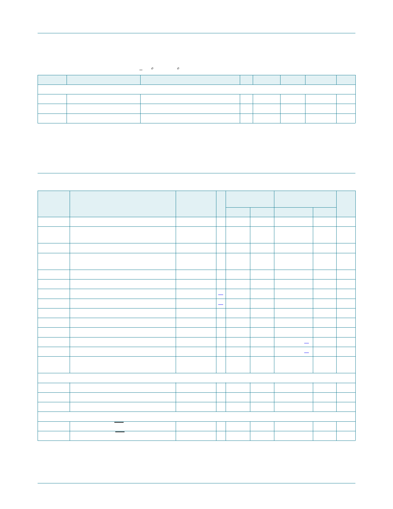
Table 10. Static characteristics …continued
VDD = 2.3 V to 5.5 V; VSS = 0 V; Tamb = 40 C to +85 C; unless otherwise specified.
Symbol Parameter
Conditions
Min
Typ
Max
Select inputs A0, A1, A2
VIL
LOW-level input voltage
0.5
-
0.8
VIH
HIGH-level input voltage
ILI
input leakage current
2.0
-
5.5
1
-
1
Unit
V
V
A
[1] VDD must be lowered to 0.2 V for at least 5 s in order to reset part.
[2] Each I/O must be externally limited to a maximum of 25 mA and the device must be limited to a maximum current of 100 mA.
[3] The total current sourced by all I/Os must be limited to 85 mA.
10. Dynamic characteristics
Table 11. Dynamic characteristics
Symbol Parameter
Conditions
fSCL
SCL clock frequency
tBUF
bus free time between a STOP and
START condition
tHD;STA
tSU;STA
hold time (repeated) START condition
set-up time for a repeated START
condition
tSU;STO
tHD;DAT
tVD;ACK
tVD;DAT
tSU;DAT
tLOW
tHIGH
tr
tf
tSP
set-up time for STOP condition
data hold time
data valid acknowledge time
data valid time
data set-up time
LOW period of the SCL clock
HIGH period of the SCL clock
rise time of both SDA and SCL signals
fall time of both SDA and SCL signals
pulse width of spikes that must be
suppressed by the input filter
Port timing
tv(Q)
data output valid time
tsu(D)
data input set-up time
th(D)
data input hold time
Interrupt timing
tv(INT_N)
trst(INT_N)
valid time on pin INT
reset time on pin INT
Standard-mode
I2C-bus
Min Max
0
100
4.7
-
Fast-mode I2C-bus Unit
Min
Max
0
400 kHz
1.3
- s
4.0
-
0.6
- s
4.7
-
0.6
- s
4.0
0
[1] 0.3
[2] 300
250
4.7
4.0
-
-
-
-
-
3.45
-
-
-
-
1000
300
50
0.6
0
0.1
50
100
1.3
0.6
20 + 0.1Cb[3]
20 + 0.1Cb[3]
-
- s
- s
0.9 s
- ns
- ns
- s
- s
300 ns
300 ns
50 ns
-
200
-
200 ns
100
-
100
- ns
1
-
1
- s
-
4
-
4 s
-
4
-
4 s
[1] tVD;ACK = time for Acknowledgement signal from SCL LOW to SDA (out) LOW.
[2] tVD;DAT = minimum time for SDA data output to be valid following SCL LOW.
[3] Cb = total capacitance of one bus line in pF.
PCA9554_9554A
Product data sheet
All information provided in this document is subject to legal disclaimers.
Rev. 10 — 8 November 2017
© NXP Semiconductors N.V. 2017. All rights reserved.
14 of 35
Share Link: 