VSC852(2000) 查看數據表(PDF) - Vitesse Semiconductor
零件编号
产品描述 (功能)
生产厂家
VSC852 Datasheet PDF : 16 Pages
| |||
VITESSE
SEMICONDUCTOR CORPORATION
Data Sheet
VSC852
1.6Gb/s 64x64
Crosspoint Switch
switch slice should connect to. The format of the program data is simple binary, where the binary value maps
directly to the switch slice position and/or input port number. For example, program data 0000100/010110
would direct output channel Y4 to connect to input channel A22.
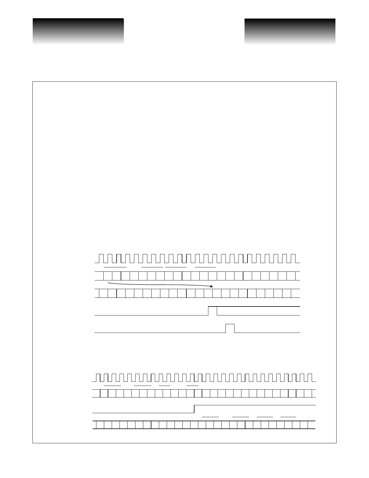
To program the switch core, the address and data (13 bits total) for the given output port must be serially
clocked into the SDIN input. The LOAD pin must be asserted with the last serial program bit to load the pro-
gram data into the on-chip program register. The program data will be held in the register until it is either repro-
grammed or the chip is powered off. The last step to programming the switch core is to transfer the program
data to the registers that control the state of each switch slice. The transfer is completed by asserting the CON-
FIG pin. The CONFIG pin can be used as a strobe to allow multiple program commands to be implemented
simultaneously. The CONFIG pin can also be tied HIGH (always asserted) so the core will reprogram after
every LOAD pulse. See Figure 1.
To read the current programming of the switch core, the desired address to query must be clocked into the
chip’s SDIN port. The format of the program data is the same as for writing. Because of the depth of the on-chip
registers, the address bits must be followed by another 6 CLK cycles so the address data is correctly positioned
in the internal register. The dummy bits that are clocked in during the last 6 bits of the program data will be
overwritten when READ is asserted. As the last dummy bit is clocked in, the READ pin must be asserted to
load the on-chip program data into the shift register used for the serial interface logic. See Figure 2.
Figure 1: Write Sequence Timing
Figure 2: Read Sequence Timing
G52245-0, Rev 4.1
9/26/00
© VITESSE SEMICONDUCTOR CORPORATION • 741 Calle Plano • Camarillo, CA 93012
Tel: (800)-VITESSE • FAX: (805) 987-5896 • Email: prodinfo@vitesse.com
Internet: www.vitesse.com
Page 3
Share Link: 