LT1374CFE 查看數據表(PDF) - Linear Technology
零件编号
产品描述 (功能)
生产厂家
LT1374CFE Datasheet PDF : 32 Pages
| |||
LT1374
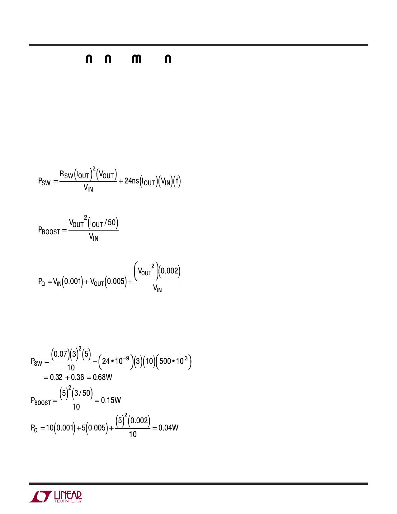
APPLICATIONS INFORMATION
THERMAL CALCULATIONS
Power dissipation in the LT1374 chip comes from four
sources: switch DC loss, switch AC loss, boost circuit
current, and input quiescent current. The following formu-
las show how to calculate each of these losses. These
formulas assume continuous mode operation, so they
should not be used for calculating efficiency at light load
currents.
Switch loss:
Boost current loss:
Quiescent current loss:
RSW = Switch resistance (≈ 0.07)
24ns = Equivalent switch current/voltage overlap time
f = Switch frequency
Example: with VIN = 10V, VOUT = 5V and IOUT = 3A:
Total power dissipation is 0.68 + 0.15 + 0.04 = 0.87W.
Thermal resistance for LT1374 package is influenced by
the presence of internal or backside planes. With a full
plane under the 16-lead TSSOP package, thermal resis-
tance will be about 40°C/W. To calculate die temperature,
use the proper thermal resistance number for the desired
package and add in worst-case ambient temperature:
TJ = TA + θJA (PTOT)
With the TSSOP16 package (θJA = 40°C/W), at an ambient
temperature of 50°C,
TJ = 50 + 40 (0.87) = 85°C
For the DD package with a good copper plane under the
device, thermal resistance will be about 30°C/W. For the
conditions above:
TJ = 50 + 30 (0.87) = 76°C
Die temperature is highest at low input voltage, so use
lowest continuous input operating voltage for thermal
calculations.
FREQUENCY COMPENSATION
Loop frequency compensation of switching regulators
can be a rather complicated problem because the reactive
components used to achieve high efficiency also intro-
duce multiple poles into the feedback loop. The inductor
and output capacitor on a conventional step-down con-
verter actually form a resonant tank circuit that can exhibit
peaking and a rapid 180° phase shift at the resonant
frequency. By contrast, the LT1374 uses a “current mode”
architecture to help alleviate phase shift created by the
inductor. The basic connections are shown in Figure 9.
Figure 10 shows a Bode plot of the phase and gain of the
power section of the LT1374, measured from the VC pin to
the output. Gain is set by the 5.3A/V transconductance of
the LT1374 power section and the effective complex
impedance from output to ground. Gain rolls off smoothly
above the 600Hz pole frequency set by the 100µF output
capacitor. Phase drop is limited to about 70°. Phase
recovers and gain levels off at the zero frequency (≈16kHz)
set by capacitor ESR (0.1Ω).
1374fd
21
Share Link: 