LTC692(Rev0) 查看數據表(PDF) - Linear Technology
零件编号
产品描述 (功能)
生产厂家
LTC692 Datasheet PDF : 16 Pages
| |||
LTC692/LTC693
APPLICATI S I FOR ATIO
VHYSTERESIS
=
5V R1
R3
=
850mV
R3 ≈ 5.88 R1
Choose R3 = 300k and R1 = 51k. Also select R4 = 10k
which is much smaller than R3.
7.25V
= 1.3V
1+5R1k2
–
(5V – 1.3V)51k
1.3V(310k)
R2 = 10.1k, Choose nearest 5% resistor 10k and recalcu-
late VL,
VL
=
1.3V 1+
51k
10 k
–
(5V – 1.3V)51k
1.3V(310k)
=
7.32V
VH
=
1.3V 1+
51k
10k
+
51k
300k
=
8.151V
(7.32V – 6.25V) = 10.7ms
100mV/ms
VHYSTERESIS = 8.151V – 7.32V = 831mV
The 10.7ms allows enough time to execute shutdown
procedure for microprocessor and 831mV of hysteresis
would prevent PFO from going low due to the noise of VIN.
Example 2: The circuit in Figure 9 can be used to measure
the regulated 5V supply to provide early warning of power
failure. Because of variations in the PFI threshold, this
circuit requires adjustment to ensure the PFI comparator
trips before the reset threshold is reached. Adjust R5 such
that the PFO output goes low when the VCC supply reaches
the desired level (e.g., 4.6V).
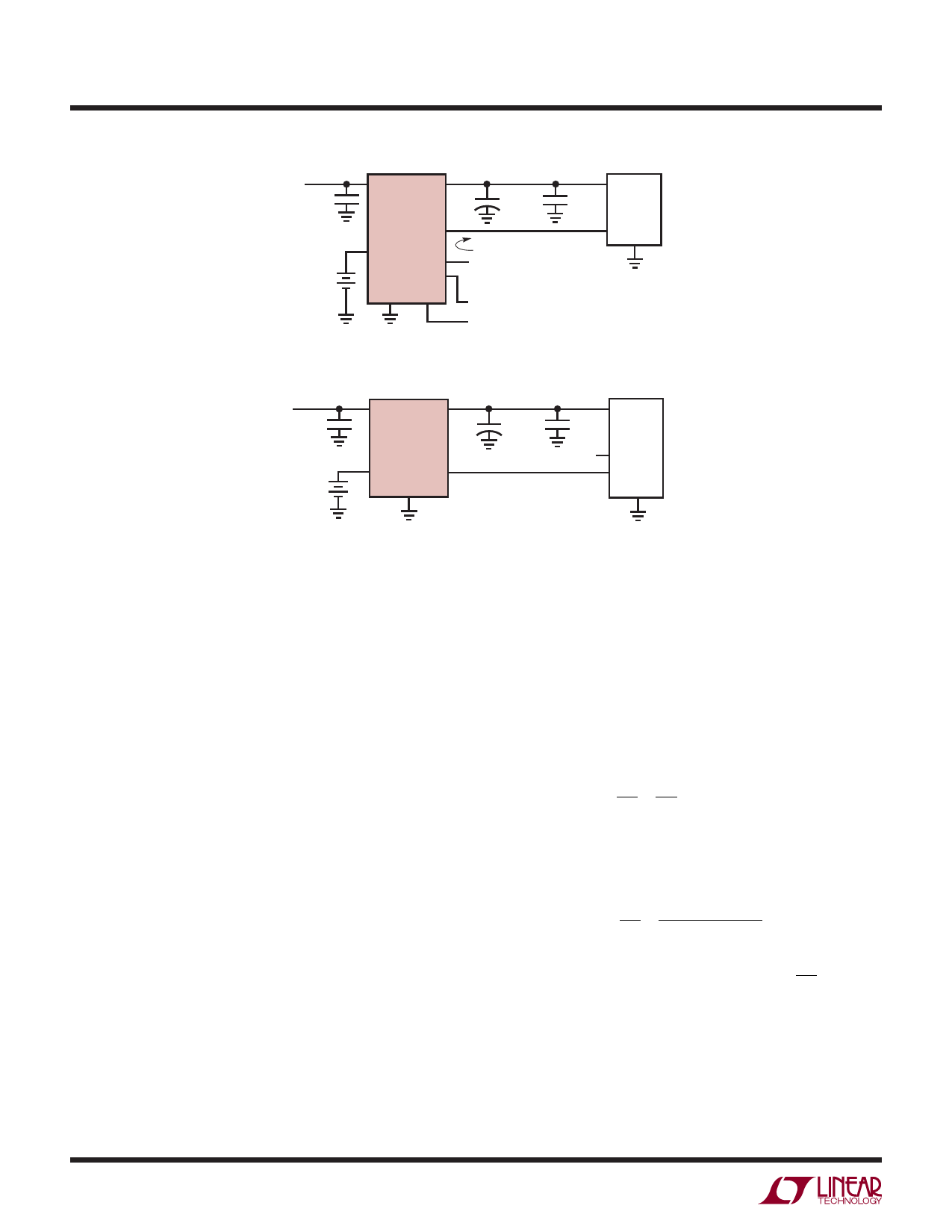
Monitoring the Status of the Battery
C3 can also monitor the status of the memory backup
battery (Figure 10). If desired, the CE OUT can be used to
apply a test load to the battery. Since CE OUT is forced high
in battery backup mode, the test load will not be applied to
the battery while it is in use, even if the microprocessor is
not powered.
5V
VBATT VCC
PFO
R1
1M
PFI LTC693
3V
R2
1M
CE IN
CE OUT GND
RL
20K
OPTIONAL TEST LOAD
LOW BATTERY SIGNAL
TO µP I/O PIN
I/O PIN
LTC692/3 • F10
Figure 10. Backup Battery Monitor with Optional Test Load
Watchdog Timer
The LTC692/LTC693 provide a watchdog timer function to
monitor the activity of the microprocessor. If the micro-
processor does not toggle the Watchdog Input (WDI)
within a seleced time-out period, RESET is forced to active
low for a minimum of 140ms. The reset active time is
adjustable on the LTC693. Since many systems cannot
service the watchdog timer immediately after a reset, the
LTC693 has longer time-out period (1.0 second mini-
mum) right after a reset is issued. The normal time-out
period (70ms minimum) becomes effective following the
first transition of WDI after RESET is inactive. The watch-
dog time-out period is fixed at a 1.0 second minimum on
the LTC692. Figure 11 shows the timing diagram of
watchdog time-out period and reset active time. The
watchdog time-out period is restarted as soon as RESET
is inactive. When either a high-to-low or low-to-high
transition occurs at the WDI pin prior to time-out, the
watchdog timer is reset and begins to time-out again. To
ensure the watchdog timer does not time-out, either a
high-to-low or low-to-high transition on the WDI pin must
occur at or less than the minimum time-out period. If the
input to the WDI pin remains either high or low, reset
pulses will be issued every 1.6 seconds typically. The
watchdog timer can be deactivated by floating the WDI pin.
The timer is also disabled when VCC falls below the reset
voltage threshold or VBATT.
12
Share Link: 