AD8801 查看數據表(PDF) - Analog Devices
零件编号
产品描述 (功能)
生产厂家
AD8801 Datasheet PDF : 16 Pages
| |||
AD8801/AD8803
OCTAL 8-BIT TRIMDAC, WITH SHUTDOWN
1
SDI
A2 A1 A0 D7 D6 D5 D4 D3 D2 D1 D0
0
1
CLK
0
1
CS
0
+5V
VOUT
0V
DAC REGISTER LOAD
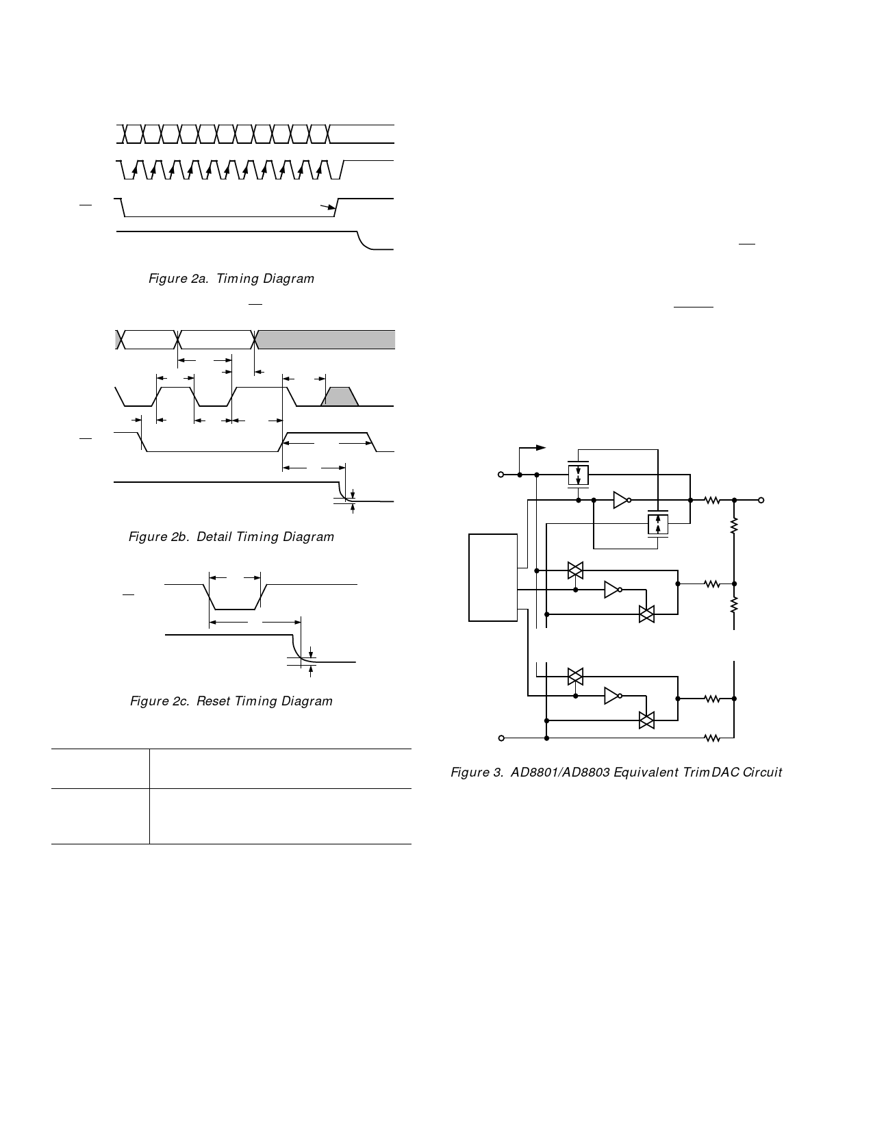
Figure 2a. Timing Diagram
DETAIL SERIAL DATA INPUT TIMING (RS = "1")
SDI 1
(DATA
IN) 0
1
CLK
0
1
CS
0
+5V
VOUT
0V
AX OR DX
tCH
AX OR DX
tDS
tDH
tCS1
tCSS
tCL
tCSH
tCSW
tS
±1 LSB ERROR BAND
±1 LSB
Figure 2b. Detail Timing Diagram
RESET TIMING
1
RS
0
+5V
VOUT
2.5V
tRS
tS
±1 LSB ERROR BAND
±1 LSB
Figure 2c. Reset Timing Diagram
Table I. Serial-Data Word Format
ADDR
DATA
B10 B9 B8 B7 B6 B5 B4 B3 B2 B1 B0
A2 A1 A0 D7 D6 D5 D4 D3 D2 D1 D0
MSB
LSB MSB
LSB
210 29 28 27 26 25 24 23 22 21 20
OPERATION
The AD8801/AD8803 provides eight channels of programmable
voltage output adjustment capability. Changing the programmed
output voltage of each TrimDAC is accomplished by clocking in
an 11-bit serial data word into the SDI (Serial Data Input) pin.
The format of this data word is three address bits, MSB first,
followed by eight data bits, MSB first. Table I provides the se-
rial register data word format. The AD8801/AD8803 has the
following address assignments for the ADDR decode which de-
termines the location of DAC register receiving the serial regis-
ter data in bits B7 through B0:
DAC # = A2 × 4 + A1 × 2 + A0 + 1
DAC outputs can be changed one at a time in random se-
quence. The fast serial-data loading of 33 MHz makes it possible
to load all eight DACs in as little time as 3 µs (12 × 8 × 30 ns).
The exact timing requirements are shown in Figure 2.
The AD8801 offers a midscale preset activated by the RS pin
simplifying initial setting conditions at first power up. The
AD8803 has both a VREFH and a VREFL pin to establish indepen-
dent positive full-scale and zero-scale settings to optimize reso-
lution. Both parts offer a power shutdown SHDN that places
the DAC structure in a zero power consumption state resulting
in only leakage currents being consumed from the power supply,
VREF inputs, and all 8 outputs. In shutdown mode the DACx
latch settings are maintained. When returning to operational
mode from power shutdown the DAC outputs return to their
previous voltage settings.
TO OTHER DACS
VREFH
P CH
N CH
MSB
2R
OX
DAC
REGISTER
D7
D6
D0
... ...
R
2R
R
...
LSB
2R
GND
2R
VREFL
Figure 3. AD8801/AD8803 Equivalent TrimDAC Circuit
PROGRAMMING THE OUTPUT VOLTAGE
The output voltage range is determined by the external refer-
ence connected to VREFH and VREFL pins. See Figure 3 for a
simplified diagram of the equivalent DAC circuit. In the case of
the AD8801, its VREFL is internally connected to GND and
therefore cannot be offset. VREFH can be tied to VDD and VREFL
can be tied to GND establishing a basic rail-to-rail voltage out-
put programming range. Other output ranges are established by
the use of different external voltage references. The general
transfer equation that determines the programmed output
voltage is:
VO (Dx) = (Dx)/256 × (VREFH – VREFL) + VREFL
(1)
where Dx is the data contained in the 8-bit DACx latch.
–4–
REV. A
Share Link: 