SN74LS374N 查看數據表(PDF) - Motorola => Freescale
零件编号
产品描述 (功能)
生产厂家
SN74LS374N Datasheet PDF : 7 Pages
| |||
SN54/74LS373 • SN54/74LS374
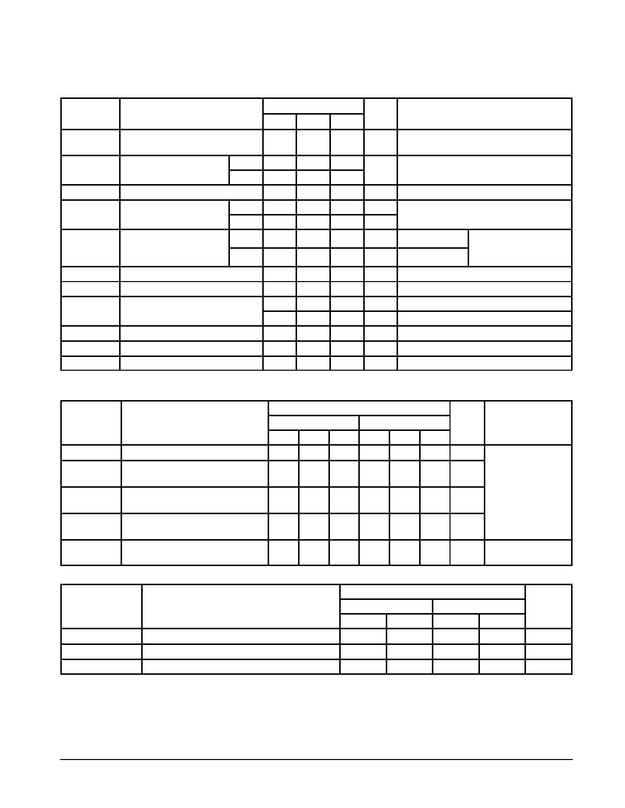
DC CHARACTERISTICS OVER OPERATING TEMPERATURE RANGE (unless otherwise specified)
Limits
Symbol
Parameter
Min Typ Max Unit
Test Conditions
VIH
Input HIGH Voltage
2.0
V
Guaranteed Input HIGH Voltage for
All Inputs
VIL
VIK
VOH
54
Input LOW Voltage
74
Input Clamp Diode Voltage
54
Output HIGH Voltage
74
0.7
0.8
– 0.65 – 1.5
2.4
3.4
2.4
3.1
Guaranteed Input LOW Voltage for
V
All Inputs
V
VCC = MIN, IIN = – 18 mA
V
VCC = MIN, IOH = MAX, VIN = VIH
V
or VIL per Truth Table
VOL
Output LOW Voltage
54, 74
74
0.25 0.4
0.35 0.5
V
IOL = 12 mA
V
IOL = 24 mA
VCC = VCC MIN,
VIN = VIL or VIH
per Truth Table
IOZH
Output Off Current HIGH
20
µA VCC = MAX, VOUT = 2.7 V
IOZL
Output Off Current LOW
– 20
µA VCC = MAX, VOUT = 0.4 V
IIH
Input HIGH Current
20
µA VCC = MAX, VIN = 2.7 V
0.1
mA VCC = MAX, VIN = 7.0 V
IIL
Input LOW Current
– 0.4 mA VCC = MAX, VIN = 0.4 V
IOS
Short Circuit Current (Note 1)
– 30
– 130 mA VCC = MAX
ICC
Power Supply Current
40
mA VCC = MAX
Note 1: Not more than one output should be shorted at a time, nor for more than 1 second.
AC CHARACTERISTICS (TA = 25°C, VCC = 5.0 V)
Limits
Symbol
Parameter
LS373
LS374
Min Typ Max Min Typ Max Unit
Test Conditions
fMAX
tPLH
tPHL
tPLH
tPHL
tPZH
tPZL
tPHZ
tPLZ
Maximum Clock Frequency
Propagation Delay,
Data to Output
Clock or Enable
to Output
Output Enable Time
Output Disable Time
35
50
MHz
12
18
12
18
ns
20
30
18
30
15
28
19
28
ns
15
28
25
36
20
28
21
28
ns
12
20
15
25
12
20
15
25
ns
CL = 45 pF,
RL = 667 Ω
CL = 5.0 pF
AC SETUP REQUIREMENTS (TA = 25°C, VCC = 5.0 V)
Limits
Symbol
Parameter
LS373
LS374
Min
Max
Min
Max
Unit
tW
Clock Pulse Width
ts
Setup Time
th
Hold Time
15
15
ns
5.0
20
ns
20
0
ns
DEFINITION OF TERMS
SETUP TIME (ts) — is defined as the minimum time required
for the correct logic level to be present at the logic input prior to
LE transition from HIGH-to-LOW in order to be recognized and
transferred to the outputs.
HOLD TIME (th) — is defined as the minimum time following
the LE transition from HIGH-to-LOW that the logic level must
be maintained at the input in order to ensure continued
recognition.
FAST AND LS TTL DATA
5-523
Share Link: 