SPT205 查看數據表(PDF) - Signal Processing Technologies
零件编号
产品描述 (功能)
生产厂家
SPT205 Datasheet PDF : 6 Pages
| |||
Current Feedback Amplifiers
Some of the key features of current feedback technology
are:
s Independence of AC bandwidth and voltage gain
s Adjustable frequency response with feedback resistor
s High slew rate
s Fast settling
Current feedback operation can be described using a simple
equation. The voltage gain for a non-inverting or inverting
current feedback amplifier is approximated by Equation 1.
Vo
Vin
=
Av
1+
Rf
Z(jω)
where:
Equation 1
s Av is the closed loop DC voltage gain
s Rf is the feedback resistor
s Z(jω) is the SPT205’s open loop transimpedance
gain
s Z(jω) is the loop gain
Rf
The denominator of Equation 1 is approximately equal to
1 at low frequencies. Near the -3dB corner frequency, the
interaction between Rf and Z(jω) dominates the circuit
performance. The value of the feedback resistor has a
large affect on the circuits performance. Increasing Rf has
the following affects:
s Decreases loop gain
s Decreases bandwidth
s Reduces gain peaking
s Lowers pulse response overshoot
s Affects frequency response phase linearity
Overdrive Protection
Unlike most other high-speed op amps, the SPT205 is not
damaged by saturation caused by overdriving input
signals (where Vin x gain > max. Vo). The SPT205 self
limits the current at the inverting input when the output is
saturated (see the inverting input current self limit
specification); this ensures that the amplifier will not be
damaged due to excessive internal currents during overdrive.
For protection against input signals which would exceed
either the maximum differential or common mode input
voltage, the diode clamp circuits below may be used.
differential protection
Vin
+Vcc
+
SPT205
Vo
-Vcc
-
Rg
common mode
protection
Figure 1: Diode Clamp Circuits for Common Mode
and Differential Mode Protection
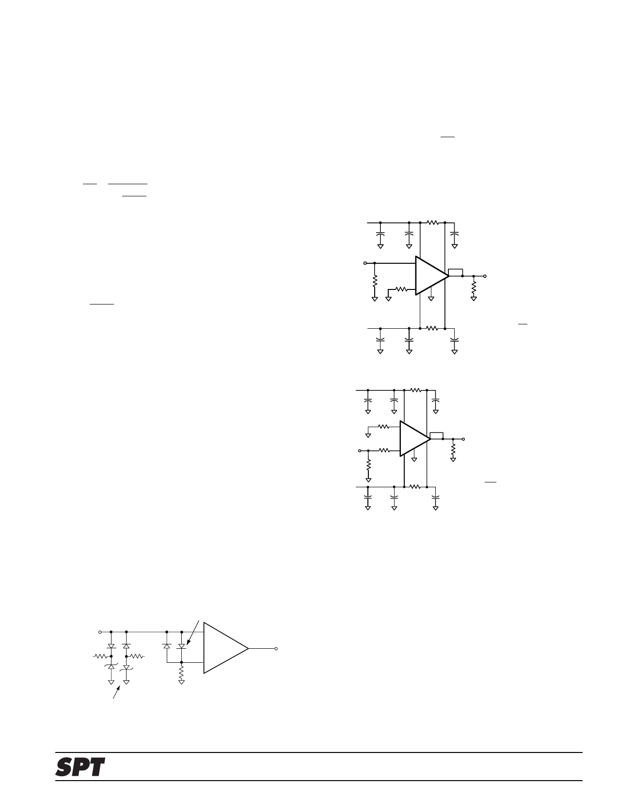
Short Circuit Protection
Damage caused by short circuits at the output may be
prevented by limiting the output current to safe levels. The
most simple current limit circuit calls for placing resistors
between the output stage collector supplies and the
output stage collectors (pins 12 and 10). The value of this
resistor is determined by:
RC
=
VC
II
− RI
where II is the desired limit current and RI is the minimum
expected load resistance (0Ω for a short to ground).
Bypass capacitors of 0.01µF on should be used on the
collectors as in Figures 2 and 3.
+15V
3.9
33Ω
Capactance in µF
.1
.01
Vin
Ri
50Ω
61
+ 12 8
SPT205
5-
10
3,7
Rg
9
11
Vo
200Ω
-15V
33Ω
3.9 .1
Av
= 1+ Rf
Rg
.01
Rf = 2000Ω (internal)
Figure 2: Recommended Non-Inverting Gain Circuit
+15V
3.9
33Ω
Capactance in µF
.1
.01
Vin
-15V
50Ω
6
1
+
12 8
Rg
Ri
SPT205
5-
10
3,7
9
11
Vo
200Ω
33Ω
3.9 .1
Av
=
-Rf
Rg
.01 Rf = 2000Ω (internal)
For Zin = 50Ω, select Rg||Ri = 50Ω
Figure 3: Recommended Inverting Gain Circuit
A more sophisticated current limit circuit which provides a
limit current independent of RI is shown in Figure 4 on
page 5.
With the component values indicated, current limiting
occurs at 50mA. For other values of current limit (II), select
RC to equal Vbe/lI. Where Vbe is the base to emitter
voltage drop of Q3 (or Q4) at a current of [2VCC – 1.4] / Rx,
where Rx ≤ [(2VCC – 1.4) / II]
Bmin. Also, Bmin is the minimum beta of Q1 (or Q2) at a
current of II. Since the limit current depends on Vbe, which
is temperature dependent, the limit current is likewise
temperature dependent.
SPT205
4
10/9/98
Share Link: 