SPT205 查看數據表(PDF) - Signal Processing Technologies
零件编号
产品描述 (功能)
生产厂家
SPT205 Datasheet PDF : 6 Pages
| |||

+Vcc
Rc
12Ω
Q1
(MJE170)
Q3
(2N3906)
to pin 12
to pin 10
0.01ΩF
Rx
14.3kΩ
0.01ΩF
Q2
(MJE180)
Rc
12Ω
Q4
(2N3904)
-Vcc
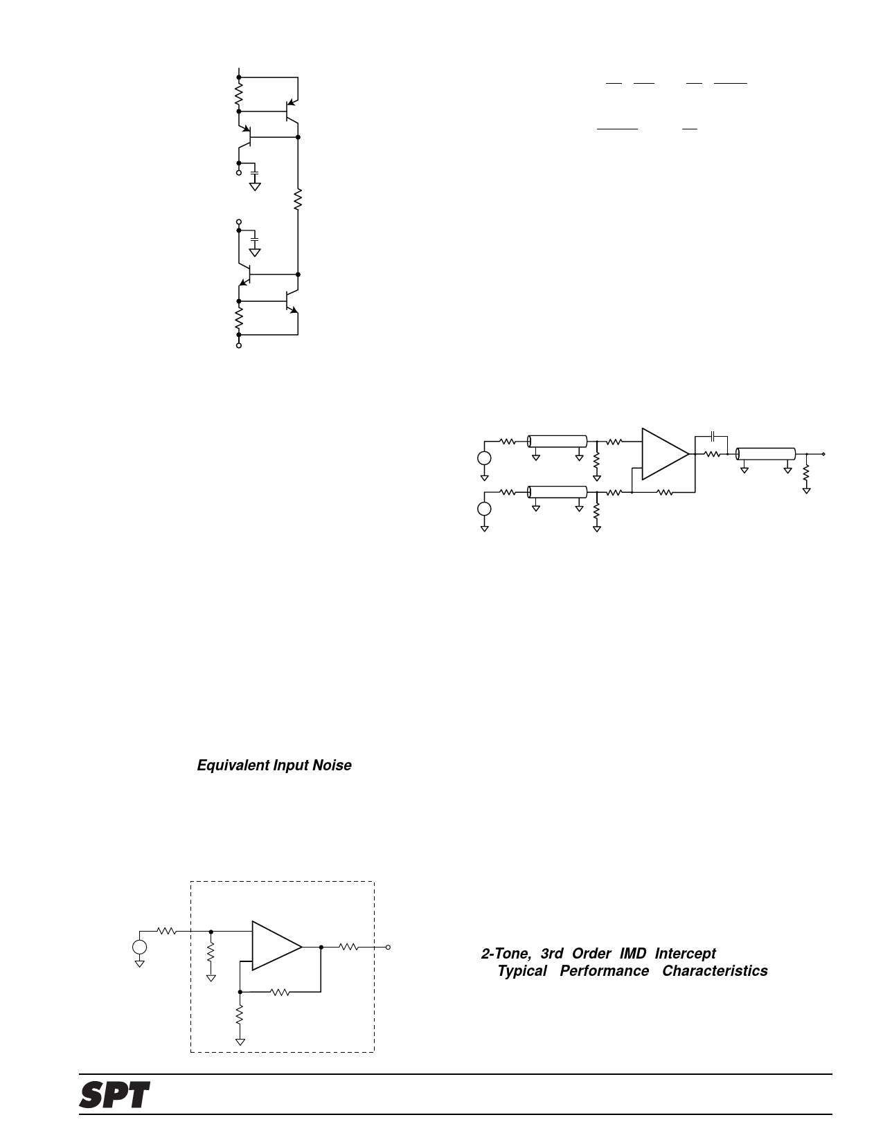
Figure 4: Active Current Limit Circuit (50mA)
Controlling Bandwidth and Passband Response
In most applications, a feedback resistor value of 2kΩ
will provide optimum performance; nonetheless, some
applications may require a resistor of some other value.
The response versus Rf plot on the previous page shows
how decreasing Rf will increase bandwidth (and frequency
response peaking, which may lead to instability). Con-
versely, large values of feedback resistance tend to roll off
the response.
F
= 10log
1+
Rs
Rn
+
Rs
4kT
⋅ in2
+
Vn2
Rp2
+
R2f ii2
Rp2
A
2
v
where Rp
+
Rs Rn
Rs + Rn
;
Av
=
Rf
Rg
+1
Figure 5: Noise Figure Diagram and Equations
(Noise Figure is for the Network Inside this Box.)
Driving Cables and Capacitive Loads
When driving cables, double termination is used to
prevent reflections. For capacitive load applications, a
small series resistor at the output of the SPT205 will
improve stability and settling performance.
Transmission Line Matching
One method for matching the characteristic impedance
(Zo) of a transmission line or cable is to place the
appropriate resistor at the input or output of the amplifier.
Figure 6 shows typical inverting and non-inverting circuit
configurations for matching transmission lines.
R1
Z0
R3
C6
+
Z0
Vo
V1 +-
R2
SPT205
-
R6
R7
R4
Z0
Rg
Rf
V2 +-
R5
Figure 6: Transmission Line Matching
The best settling time performance requires the use of an
external feedback resistor (use of the internal resistor
results in a 0.1% to 0.2% settling tail). The settling
performance may be improved slightly by adding a ca-
pacitance of 0.4pF in parallel with the feedback
resistor (settling time specifications reflect performance
with an external feedback resistor but with no external
capacitance).
Noise Analysis
Approximate noise figure can be determined for the
SPT205 using the Equivalent Input Noise plot on page 3
and the equations shown below.
kT = 4.00 x 10⁻²¹ Joules at 290°K
Vn is spot noise voltage (V/√Hz)
in is non-inverting spot noise current (A/√Hz)
ii is inverting spot noise current (A/√Hz)
Non-inverting gain applications:
s Connect Rg directly to ground.
s Make R1, R2, R6, and R7 equal to Zo.
s Use R3 to isolate the amplifier from reactive
loading caused by the transmission line,
or by parasitics.
Inverting gain applications:
s Connect R3 directly to ground.
s Make the resistors R4, R6, and R7 equal to Zo.
s Make R5 II Rg = Zo.
The input and output matching resistors attenuate the
signal by a factor of 2, therefore additional gain is needed.
Use C6 to match the output transmission line over a
greater frequency range. C6 compensates for the increase
of the amplifier’s output impedance with frequency.
Rs
+
Ro
Rn
SPT205
-
Rf
Rg
Dynamic Range (Intermods)
For RF applications, the SPT205 specifies a third
order intercept of 30dBm at 60MHz and Po = 10dBm.
A 2-Tone, 3rd Order IMD Intercept plot is found in
the Typical Performance Characteristics section.
The output power level is taken at the load. Third-order
harmonic distortion is calculated with the
formula:
HD3rd = 2 • (IP3o – Po)
SPT205
5
10/9/98