WM8181 查看數據表(PDF) - Wolfson Microelectronics plc
零件编号
产品描述 (功能)
生产厂家
WM8181 Datasheet PDF : 14 Pages
| |||
Advanced Information
DEVICE DESCRIPTION
WM8181
INTRODUCTION
The WM8181 is a serial output ADC that is designed to digitise analogue signals directly from CIS
and CCD sensors. The reset or reference level and video level from the sensor outputs are sampled
using an internal Sample and Hold circuit with an optional black level Clamp. The difference between
the sampled levels is passed onto a pipeline ADC with internally generated references where it is
converted into a 12-bit digital output. Please refer to the block diagram shown on page 1.
GENERAL OPERATION
SAMPLE AND HOLD
The WM8181 Sample and Hold samples signals from the VINP and VINM inputs. VINM and VINP
are connected to the sensor video output and a black level reference. No external buffering is
required as long as the input signals have settled before the samples are taken. The black level
reference can be provided by either the sensor or a separate circuit. Both inputs are sampled
simultaneously and the difference is passed on to the ADC to be converted.
For positive-going sensor outputs, VINP is used to input the video signal and VINM is used as the
black level reference. For negative-going sensor outputs, VINM is used as the video input and VINP
is used as the black level reference.
CLAMP
For a.c. (capacitively) coupled CCD signals, VINP and VINM may be connected together via the
optional internal clamp switch, which is controlled by the CLAMP pin. The switch is closed during the
reset period of the sensor output and open during the video period, allowing reset level clamping to
be performed. This ensures that the input signal is maintained within the input voltage limits of the
device, and that the true value of the video signal is processed.
ADC
The ADC converts the differential output from the Sample and Hold into 12-bit digital data ensuring
no missing codes in the final digitised output. The 12-bit parallel output from the ADC is transformed
into serial format, which is available to the user at the DOUT pin, MSB first.
REFERENCES
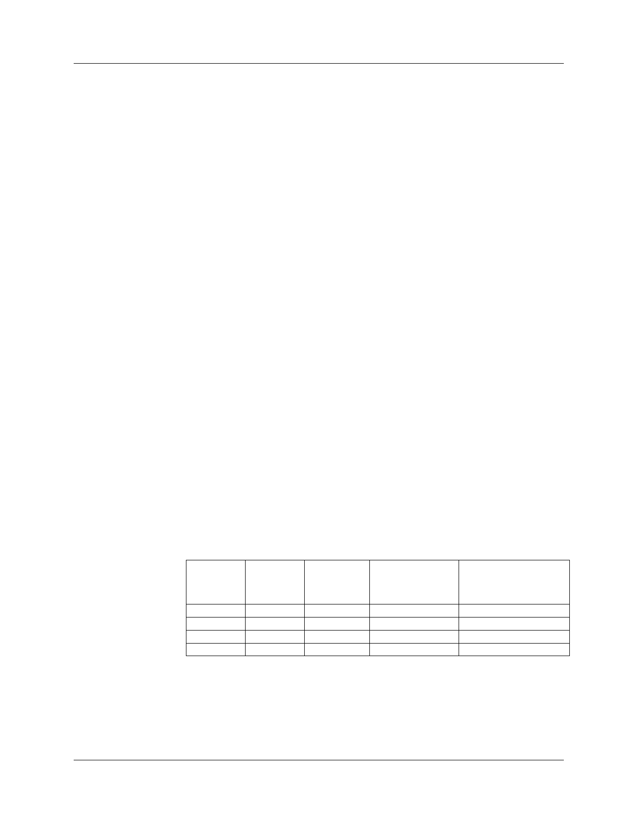
The WM8181 has internally generated references, which are controlled via the VREFIN pin. These
references are used to set the upper (VRT) and lower limits (VRB) of the ADC range and the full-
scale input range (VINP – VINM) of the device.
If VREFIN is tied to AVDD, the internal bandgap generator is used to determine the full-scale range.
If VREFIN is not tied to AVDD, the full-scale range is determined by the voltage on the VREFIN pin.
This is shown in Table 1. The ADC reference voltages, VRT and VRB, are driven onto the VRT and
VRB pins by internal amplifiers in the WM8181. Only external decoupling capacitors are required for
the VRT and VRB pins.
SUPPLY (V) VREFIN (V)
REFERENCE
CONTROL
INPUT VOLTAGE
(VINP-VINM) FOR
ZERO (0) OUTPUT
CODE
INPUT VOLTAGE (VINP-
VINM) FOR FULL-SCALE
(+4095) OUTPUT CODE
5
AVDD
Internal
0
1.5
5
0.5 - 2
External
0
VREFIN
3.3
AVDD
Internal
0
3.3
0.75 – 1.5
External
0
1.5
VREFIN
Table 1 VREFIN and ADC Input Voltage Requirements for Internal and External
Reference Control
WOLFSON MICROELECTRONICS LTD
AI Rev 3.0 January 2000
7
Share Link: 