A75 وں¥çœ‹و•¸و“ڑè،¨ï¼ˆPDF) - Intel
零ن»¶ç¼–هڈ·
ن؛§ه“پوڈڈè؟° (هٹں能)
ç”ںن؛§هژ‚ه®¶
A75 Datasheet PDF : 70 Pages
| |||
E
PENTIUMآ® PROCESSOR 75/90/100/120/133/150/166/200
Pentiumآ® Processor (75/90/100/120/133/150/166/200 MHz)
Control
DP
Logic
Branch
Target
Buffer
TLB
Prefetch
Address
Code Cache
8 KBytes
64-Bit
Data
Bus
Instruction
Pointer
Branch Verification
and Target Address
256
Prefetch Buffers
Instruction Decode
Control Unit
32-Bit
Address Bus
Bus
Unit
Control
Page
Unit
64-Bit
Data
Bus
64
32
32-Bit
Addr.
Bus
Data
Control
APIC
Address
Generate
(U Pipeline)
Address
Generate
(V Pipeline)
Integer Register File
ALU
ALU
(U Pipeline) (V Pipeline)
Barrel Shifter
32
Data Cache
32
32
8 KBytes
TLB
32
32
32
Control
ROM
Floating
Point
Unit
Control
Register File
Add
Divide
80
Multiply
80
199718
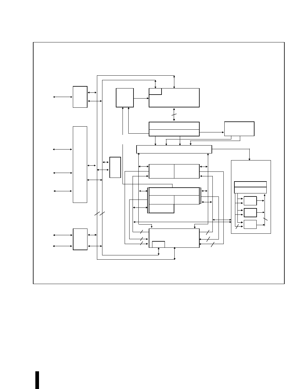
Figure 1. Pentiumآ® Processor Block Diagram
The block diagram shows the two instruction
pipelines, the "u†pipe and the "v†pipe. The u-pipe
can execute all integer and floating point
instructions. The v-pipe can execute simple integer
instructions and the FXCH floating-point
instructions.
The separate code and data caches are shown.
The data cache has two ports, one for each of the
two pipes (the tags are triple ported to allow
simultaneous inquire cycles). The data cache has
a dedicated Translation Lookaside Buffer (TLB) to
translate linear addresses to the physical
addresses used by the data cache.
The code cache, branch target buffer and prefetch
buffers are responsible for getting raw instructions
into the execution units of the Pentium processor.
Instructions are fetched from the code cache or
from the external bus. Branch addresses are
remembered by the branch target buffer. The code
cache TLB translates linear addresses to physical
addresses used by the code cache.
5
Share Link: 