IN74HC4046AD 查看數據表(PDF) - Integral Corp.
零件编号
产品描述 (功能)
生产厂家
IN74HC4046AD Datasheet PDF : 11 Pages
| |||
IN74HC4046A
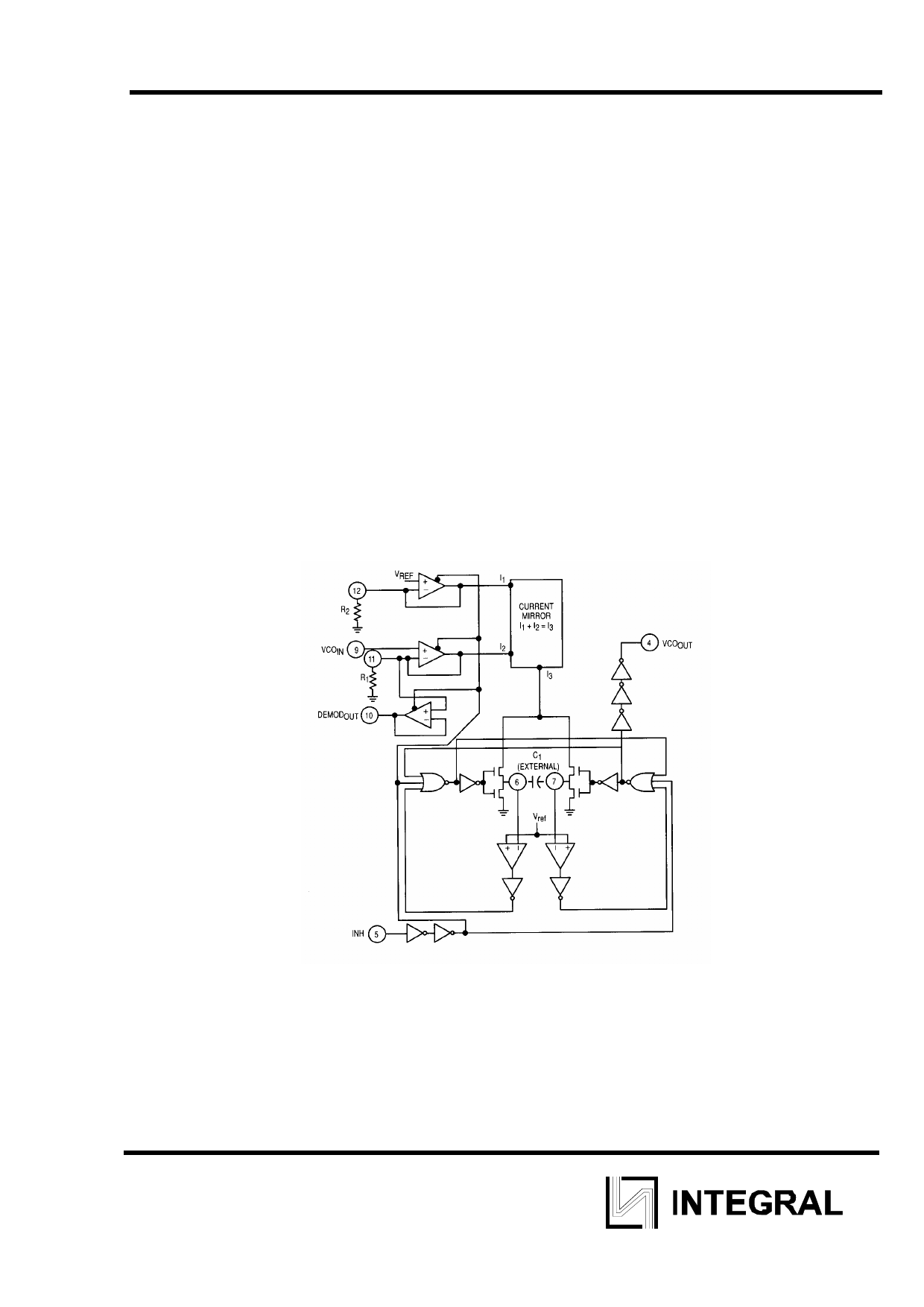
DETAILED CIRCUIT DESCRIPTION
Voltage Controlled Oscillator/Demodulator
Output
The VCO requires two or three external
components to operate. These are R1, R2, C1.
Resistor R1 and Capacitor C1 are selected to
determine the center frequency of the VCO (see
typical performance curves Figure 12). R2 can be
used to set the offset frequency with 0 volts at
VCO input. For example, if R2 is decreased, the
offset frequency is increased. If R2 is omitted the
VCO range is from 0 Hz. By increasing the value
of R2 the lock range of the PLL is increased and
the gain (volts/Hz) is decreased. Thus, for a
narrow lock range, large swings on the VCO input
will cause less frequency variation.
Internally, the resistors set a current in a
current mirror, as shown in Figure 5. The mirrored
current drives one side of the capacitor. Once the
voltage across the capacitor charges up to Vref of
the comparators, the oscillator logic flips the
capacitor which causes the mirror to change the
opposite side of the capacitor. The output from
the internal logic is then taken to VCO output
(Pin4).
The input to the VCO is a very high
impedance CMOS input and thus will not load
down the loop filter, easing the filters design. In
order to make signals at the VCO input accessible
without degrading the loop performance, the VCO
input voltage is buffered through a unity gain Op-
amp, to Demod Output. This Op-amp can drive
loads of 50K ohms or more and provides no
loading effects to the VCO input voltage (see
Figure 10).
An inhibit input is provided to allow
disabling of the VCO and all Op-amps (see Figure
5). This is useful if the internal VCO is not being
used. A logic high on inhibit disables the VCO and
all Op-amps, minimizing standby power
consumption.
The output of the VCO is a standard high speed
CMOS output with an equivalent LS-TTL fan out
of 10. The VCO output is approximately a square
wave. This output can either directly feed the
COMPIN of the phase comparators or feed
external prescalers (counters) to enable
frequency synthesis.
Figure 5. Logic Diagram for VCO
Phase Comparators
All three phase comparators have two inputs,
SIGIN and COMPIN. The SIGIN and COMPIN have
a special DC bias network that enables AC
coupling of input signals. If the signals are not AC
coupled, standard IN74HC input levels are
required. Both input structures are shown in
Figure 6. The outputs of these comparators are
essentially standard IN74HC outputs (comparator
2 is TRI-STATEABLE). In normal operation VCC
and ground voltage levels are fed to the loop filter.
This differs from some phase detectors which
supply a current to the loop filter and should be
considered in the design.
7
Share Link: 