HC4046 查看數據表(PDF) - System Logic Semiconductor
零件编号
产品描述 (功能)
生产厂家
HC4046 Datasheet PDF : 12 Pages
| |||
SL74HC4046
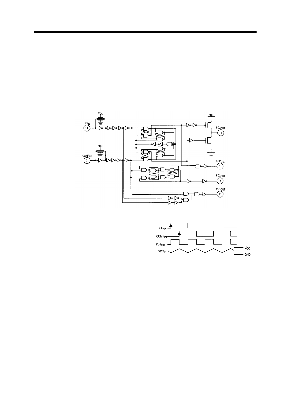
Phase Comparators
All three phase comparators have two inputs,
SIGIN and COMPIN. The SIGIN and COMPIN have a
special DC bias network that enables AC coupling of
input signals. If the signals are not AC coupled,
standard SL74HC input levels are required. Both input
structures are shown in Figure 6. The outputs of these
comparators are essentially standard SL74HC outputs
(comparator 2 is TRI-STATEABLE). In normal
operation VCC and ground voltage levels are fed to the
loop filter. This differs from some phase detectors
which supply a current to the loop filter and should be
considered in the design.
Phase Comparator 1
Figure 6. Logic Diagram for Phase Comparators
This comparator is a simple XOR gate similar to
the SL74HC86. Its operation is similar to an overdriven
balanced modulator. To maximize lock range the input
frequencies must have a 50% duty cycle. Typical input
and output waveforms are shown in Figure 7. The
output of the phase detector feeds the loop filter which
averages the output voltage. The frequency range
upon which the PLL will lock onto if initially out of lock
is defined as the capture range.The capture range for
phase detector 1 is dependent on the loop filter design.
The capture range can be as large as the lock range,
which is equal to the VCO frequency range.
To see how the detector operates, refer to
Figure 7. When two square wave signals are applied to
this comparator, an output waveform (whose duty
cycle is dependent on the phase difference between
the two signals) results. As the phase difference
increases, the output duty cycle increases and the
voltage after the loop filter increases. In order to
achieve lock when the PLL input frequency increases,
the VCO input voltage must increase and the phase
difference between COMPIN and SIGIN will increase. At
an input frequency equal to fmin, the VCO input is at 0
V
Figure 7. Typical Waveforms for PLL Using
Phase Comparator 1
This requires the phase detector output to be
grounded; hence, the two input signals must be in
phase. When the input frequency is fmax, the VCO
input must be VCC and the phase detector inputs must
be 180 degrees out of phase.
The XOR is more susceptible to locking onto
harmonics of the SIGIN than the digital phase detector
2. For instance, a signal 2 times the VCO frequency
results in the same output duty cycle as a signal equal
to the VCO frequency. The difference is that the
output frequency of the 2f example is twice that of the
other example. The loop filter and VCO range should
be designed to prevent locking on to harmonics.
488
Share Link: 