M66007FP 查看數據表(PDF) - MITSUBISHI ELECTRIC
零件编号
产品描述 (功能)
生产厂家
M66007FP Datasheet PDF : 6 Pages
| |||
MITSUBISHI 〈DIGITAL ASSP〉
M66007P/FP
12-BIT INPUT EXPANDER
PRECAUTIONS FOR APPLICATION
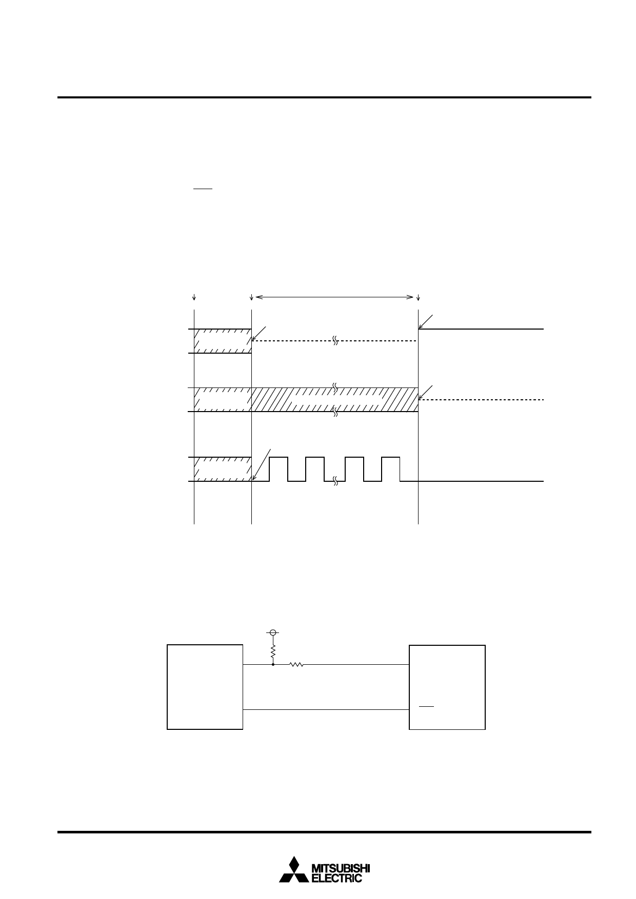
1. The following timing diagram shows the status of MCU port
and LE/D pin of the M66007 when power is turned on.
When MCU has been reset to make the collision period of
MCU and LE/D line of the M66007 as short as possible,
place the port (LE/D) in input mode and execute the reset
sequence through the port (CLK) promptly to reset the
M66007.
As shown in the diagram, to prevent the IC from being bro-
ken due to collision of the LE/D line in the 1-2 section, set
in the LE/D line in series a resistance of a degree to which
the transmission speed cannot be affected.
2. When the LE/D pin on each of the MPU and M66007 sides
switches from input mode to output mode or from output
mode to input mode, the LE/D pin may be placed in high
impedance status, resulting in oscillation.
To prevent malfunction due to this oscillation, pull up the
LE/D line with a high resistance of a degree to which VOH
and VOL levels cannot be affected. (with approx. 20kΩ pull-
up resistance built-in)
Power ON
MCU reset
M66007 reset sequence
MCU port (DATA)
Input/output
indeterminate
Input mode
M66007
RESET
Output mode
M66007 LE/D
Input/output
indeterminate
Input/output indeterminate
Input mode
MCU port (CLK)
Input/output
indeterminate
Output mode
13 clocks or more
1
2
3
Status of MCU and M66007 with Power Turned on
MCU
Port
(DATA)
Port
(CLK)
Pull-resistance
Serial resistance
I/O=LE/D
M66007
I=CLK
Connection Example of MCU and M66007
6
Share Link: 