M52342SP 查看數據表(PDF) - MITSUBISHI ELECTRIC
零件编号
产品描述 (功能)
生产厂家
M52342SP Datasheet PDF : 14 Pages
| |||
MITSUBISHI ICs (TV)
M52342SP
PLL-SPLIT VIF/SIF IC
ELECTRICAL CHARACTERISTICS TEST METHOD
Video S/N
Input SG2 into VIF IN and measure the video out (Pin 18) noise in
r.m.s at TP18B through a 5MHz (-3dB) L.P.F.
S/N=20 log 0.7×Vo det (dB)
NOISE
BW Video band width
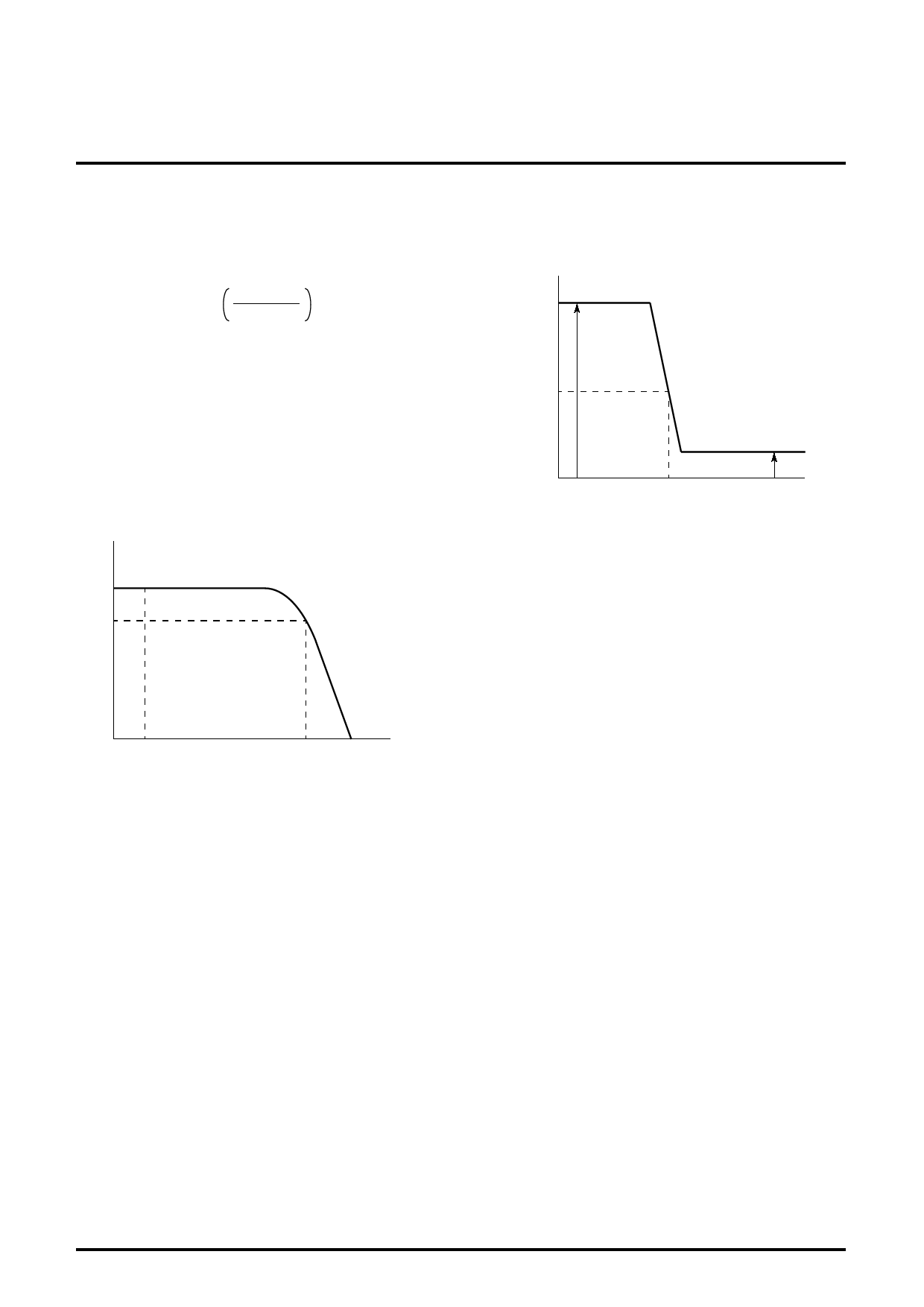
1. Measure the 1MHz component level of EQ output TP18A with a
spectrum analyzer when SG3 (f2=57.75MHz) is input into VIF
IN. At that time, measure the voltage at TP8 with SW8, set to
position 2, and then fix V8 at that voltage.
2. Reduce f2 and measure the value of (f2-f0) when the (f2-f0)
component level reaches -3dB from the 1MHz component level
as shown below.
TP18
-3dB
V3 RF AGC operating voltage
Input SG8 into VIF IN, and gradually reduce Vi and then measure
the input level when RF AGC output TP3 reaches 1/2 VCC, as
shown below.
TP3
Voltage
V3H
1/2VCC
V3L
Vi
Vi (dBµ)
CL-U Capture range
1. Increase the frequency of SG9 until the VCO is out of locked-
oscillation.
2. Decrease the frequency of SG9 and measure the frequency fU
when the VCO locks.
CL-U=fU-58.75 (MHz)
1MHz
( f2 - f0 )
BW
VIN MIN Input sensitivity
Input SG4 (Vi=90dBµ) into VIF IN, and then gradually reduce Vi and
measure the input level when the 20kHz component of EQ output
TP18A reaches -3dB from Vo det level.
VIN MAX Maximum allowable input
1. Input SG5 (Vi=90dBµ) into VIF IN, and measure the level of the
20kHz component of EQ output.
2. Gradually increase the Vi of SG and measure the input level
when the output reaches -3dB.
GR AGC control range
GR=VIN MAX-VIN MIN (dB)
CL-L Capture range
1. Decrease the frequency of SG9 until the VCO is out of locked-
oscillation.
2. Increase the frequency of SG9 and measure the frequency fL
when the VCO locks.
CL-L=58.75-fL (MHz)
CL-T Capture range
CL-T=CL-U+CL-L (MHz)
µ AFT sensitivity, V2H Maximum AFT voltage, V2L Minimum AFT
voltage
1. Input SG10 into VIF IN , and set the frequency of SG10 so that
the voltage of AFT output TP2 is 3V. This frequency is named
f(3).
2. Set the frequency of SG10 so that the AFT output voltage is 2V.
This frequency is named f (2)
4
Share Link: 